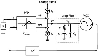
Integrated Circuit Design for High-Speed Frequency Synthesis

A charge pump is the first analog component of a synthesizer that will be considered. It is responsible for placing charge into or taking charge out of the loop filter, and, therefore, moving the control voltage on the VCO up or down, as shown in Figure 7.1. Charge pumps must be very carefully designed to minimize reference feedthrough or phase noise. In spite of numerous variations, a charge pump will usually be composed of two current sources and two switches. This chapter also deals with loop filters. Although Chapter 3 has already considered basic loop filters, a large number of modifications to improve performance can be added to the basic design.
The following sections will deal with various charge pump design issues, and circuit-level designs will be presented.
Probably one of the most basic and common charge pumps is shown in Figure 7.2. This charge pump consists of four transistors M 1 through M 4. Transistors M 1 and M 4 act as current sources, while transistors M 2 and M 3 act like switches that are controlled by the PFD. When the PFD is in the tristate, then UP must be high (at V DD), while DN must be connected low (to V SS). Note that an inverter between the PFD output and the DN or UP input of the charge pump...