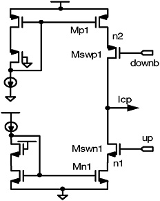
Low-Voltage CMOS RF Frequency Synthesizers

A charge pump (CP) is used to sink and source current into the loop filter based on the outputs of the PFD. A schematic of a CP is shown in Fig. 3.39. Transistors Mn1 and Mp1 provide up and down currents and are combined to generate the required net current to sink from or to source to the loop filter. The switches Mswp1 and Mswn1 are driven by the up and downb output signals of the phase frequency detector. If both the switches Mswp1 and Mswn1 are turned off, the voltages at nodes n1 and n2 are pulled to ground and V DD, respectively. When the switches are turned on again, charge disturbance is induced by the voltage difference between the output of the charge pump and the voltages at nodes n1 and n2. Ripples, therefore, occur at the output of the loop filter, which result in spurs in the synthesizer output. To remedy this, a dummy branch, which consists of switches Mswp2 and Mswn2, as shown in Fig. 3.40, can be used. Once the switches Mswp1 and Mswn1 are turned off, the switches Mswp2 and Mswn2 are turned on. Consequently, it prevents nodes n1 and n2 from being discharged and charged, respectively. Complementary switches (Mswp1 ?, Mswp2 ?, Mswn1 ? and Mswn2 ?) are used to provide complementary charges so as to minimize the error at the loop filter due to charge injection and clock feed-through.