Microcontrollers in Practice
Packed with hundreds of practical examples and exercises to foster mastery of concepts and details, this practical guide provides readers with hands-on knowledge of how to implement three families of microcontrollers.
This chapter describes a simple, yet flexible development board, based on AT90S8535, for the study of the AVR microcontrollers. This board can be used to test most of the AVR projects presented in this book.
The schematic of the development board is shown in Fig. 10.1. The circuit comprises the following functional blocks:
Microcontroller
Clock circuit
RESET circuit
Output buffers
ISP interface
RS232 interface
Power supply circuit.
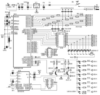
The microcontroller is an AT90S8535-P in a DIP40 package. Note that this microcontroller is pin by pin, hardware compatible with other members of the analog series of AVR microcontrollers, like ATMega8535 and ATMega16. However, there are many differences between these microcontrollers. Consult the data sheets before making the replacement.
The external clock circuit uses an 8 MHz crystal, Q1, and the capacitors C10, C11 (12 47 pF). The RESET circuit consists of the resistor R1 (10 K), and the capacitor C1 (10 F/10 V). These values are not critical, because AT90S8535 contains internal signal conditioning circuits for the RESET signal.
The digital input lines are connected to PORTC, and are pulled up to V cc with resistors. A group of LEDs has been included, to show the status of each input.
The idle status of the input lines is HIGH. An input line is active when pulled to GND (for example by the contact of a relay). In this case, the associated LED will light, indicating the...