SilicideTechnology for Integrated Circuits

This detailed text provides guidance on the development and application of metal silicide technology as it emerges from the scientific to the prototype and manufacturing stages.
 TABLE OF CONTENTS
 J.E. Burnette, M. Himmerlich and
R.J. Nemanich
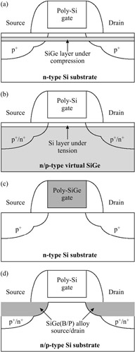
Electronic devices based on Si/Ge alloys are already important for high frequency applications [1] and infrared detectors [2]. Heterojunction bipolar transistors (HBTs) which were first reported in 1988 [3], have demonstrated operating frequencies significantly greater than 100 GHz. Moreover, the electronic properties of Si/Ge with respect to and in combination with silicon offer significant advantages for integrated circuit technology [4, 5]. Some examples of the potential of Si/Ge in CMOS technology are displayed in FIGURE 7.1. In fact, the combination of HBT and CMOS will provide the potential for monolithic silicon-based RF systems [1].
The development of ohmic or rectifying contacts to these semiconducting Si/Ge layers is a critical step in the development of the device technologies. Understanding the formation and electronic states of contacts to Si/Ge semiconducting layers begins with the clean surfaces. The formation and stability of the contacts will depend on the interface chemistry, and for Si/Ge, the system shows significant complexity in comparison to silicide contacts to silicon surfaces. Finally, the device operation will depend on the electrical properties of the interface. This chapter presents summaries...