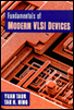
Fundamentals of Modern VLSI Devices

Chapter 2: Basic Device Physics

This chapter reviews the basic concepts of semiconductor device physics. Starting with electrons and holes and their transport in silicon, we focus on the most elementary types of devices in VLSI technology: p n junction and metal-oxide-semiconductor (MOS) capacitor. The rest of the chapter deals with subjects of importance to VLSI device reliability: high-field effects, the Si-SiO 2 system, and dielectric breakdown.

2.1 ELECTRONS AND HOLES IN SILICON

The first section covers energy bands in silicon, Fermi level, n-type and p-type silicon, electrostatic potential, drift and diffusion current transport, and basic equations governing VLSI device operation. These will serve as the basis for understanding the more advanced device concepts discussed in the rest of the book.

2.1.1 ENERGY BANDS IN SILICON

The starting material used in the fabrication of VLSI devices is silicon in the crystalline form. The silicon wafers are cut parallel to either the 111 or 100 planes (Sze, 1981), with 100 material being the most commonly used. This is largely due to the fact that 100 wafers, during processing, produce the lowest charges at the oxide-silicon interface as well as higher mobility (Balk et al., 1965). In a silicon crystal each atom has four valence electrons to share with its four nearest neighboring atoms. The valence electrons are shared in a paired configuration called a cova lent bond. The most important result of the application of quantum mechanics to the description of electrons in a solid is that the allowed energy...

UNLIMITED FREE
ACCESS
TO THE WORLD'S BEST IDEAS

SUBMIT
Already a GlobalSpec user? Log in.

This is embarrasing...

An error occurred while processing the form. Please try again in a few minutes.

Customize Your GlobalSpec Experience

Category: Semiconducting Materials
Finish!
Privacy Policy

This is embarrasing...

An error occurred while processing the form. Please try again in a few minutes.