Fundamentals of Modern VLSI Devices

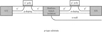
A more or less generic CMOS process flow is described below. It features shallow trench isolation (STI) (Davari et al., 1988b, 1989), dual n +/p + polysilicon gates (Wong et al., 1988; Sun et al., 1989), and self-aligned silicide (Ting et al., 1982). The front-end-of-the-line process consists of six or seven masking levels and is suitable for sub-0.5- m generations of VLSI logic and SRAM technology.
Starting material p-type substrate or p epi on p + substrate for latch-up prevention (Taur et al., 1984).
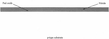
Grow pad oxide. Deposit CVD (Chemical Vapor Deposition) nitride. (See Fig. A1.1.)
FIGURE A1.1
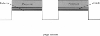
Lithography to cover the active region with photoresist.
Reactive ion etching (RIE) nitride and oxide in the field region.
RIE shallow trench in silicon. (See Fig. A1.2.)
FIGURE A1.2
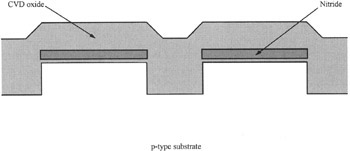
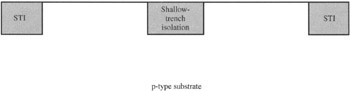
Grow pad oxide. Deposit thick CVD oxide. (See Fig. A1.3)
FIGURE A1.3
Chemical-mechanical polishing planarization. (See Fig. A1.4)
FIGURE A1.4
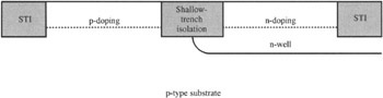
n-well lithography and implant (also channel doping).
p-well lithography and implant (also channel doping). (See Fig. A1.5.)
FIGURE A1.5
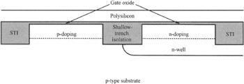
Grow gate oxide.
Deposit polysilicon film. (See Fig. A1.6.)
FIGURE A1.6
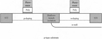
Gate lithography.
RIE polysilicon gate. (See Fig. A1.7.)
FIGURE A1.7
Sidewall reoxidation.
n + source-drain lithography and implant (also dope n + polysilicon gate).
p + source-drain lithography and implant (also dope p + polysilicon gate). (See Fig. A1.8.)
FIGURE A1.8
Oxide (or nitride) spacer...