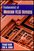
Fundamentals of Modern VLSI Devices

In the presence of an electric field, carriers gain energy from the field as they drift along. These carriers in turn lose energy by emitting phonons. As the field increases, the average energy of the carriers increases. At sufficiently high fields, a number of physical phenomena which have important implications on the design and operation of VLSI devices can occur. In the case of high fields in silicon, these phenomena include impact ionization, or generation of electron-hole pairs; junction breakdown; band-to-band tunneling; and injection of hot carriers from locations near the silicon-oxide interface into the silicon dioxide region. In the case of high fields in silicon dioxide, the important phenomena include tunneling through the oxide layer and dielectric breakdown. The basic physics of these phenomena as they relate to VLSI devices is discussed in this section.
Consider the depletion region of a p n diode. At sufficiently high fields, an electron in the conduction band can gain enough energy to lift an electron from the valence band into the conduction band, thus generating one free electron in the conduction band and one free hole in the valence band. This process is known as impact ionization. Similarly, a hole in the valence band can gain enough energy to cause impact ionization. If the field is high enough, these secondary electrons and holes can themselves cause further impact ionization, thus beginning a process of carrier multiplication in the high-field region. The p n diode...