Fundamentals of Modern VLSI Devices

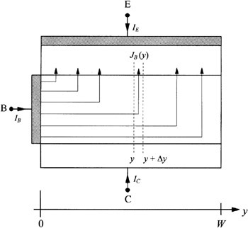
Consider the intrinsic part of a bipolar transistor, the cross section of which is shown schematically in Fig. A9.1. The base current I B enters the intrinsic-base region at the base contact and then spreads out, turns upward, and enters the emitter. Thus, the effective intrinsic-base resistance r bi as seen by the base current depends on how the base current spreads out inside the intrinsic-base layer. One commonly used method for evaluating r bi is to consider the power dissipation P in the intrinsic base (Hauser, 1968), and define r bi by
| (A9.1) | |
The power dissipation can be evaluated readily for low-current situations where there is no current crowding and the base-current density J B entering the emitter can be assumed to be uniform. That this is a good assumption for modern bipolar transistors will be shown later.
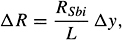
Let us assume the emitter stripe has a width W and a length L, and the base is contacted on one side of the emitter only, as shown in Fig. A9.1. Consider a slice of the intrinsic base between points y and y+ ? y. The resistance of this slice as seen by the base current is
| (A9.2) | |
where R