Small Signal Amplifier Design: A Collection from Applied Microwave & Wireless
Understanding the effects of package inductance and capacitance helps you specify the right device for your application
By Oleksandr Gorbachov
From APPLIED MICROWAVE & WIRELESS, VOL. 11, NO. 4, APRIL 1999
At microwaves, the parasitic parameters of a package have a significant influence on the main output parameters of the semiconductor devices, such as diodes or transistors. But usually designers and users of these devices employ a simplified approach to the choice of a package, considering only a lumpedelement equivalent circuit without comparing their values confirmed to the individual parts of the real package. This can result in the choice of the incorrect package, and as a consequence, to a significant deterioration of operational parameters of the semiconductors. The work described in this article is an attempt to develop a suitable calculation approach to estimate the parasitic parameters of microwave transistor packages as accurately as possible.
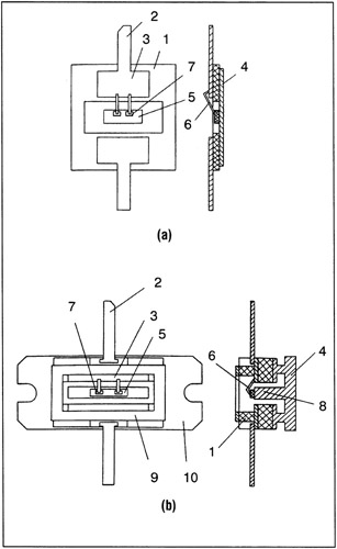
The calculations were made for the low-cost RA ceramic package (Figure 1(a)) used for a wide class of L-band GaAs FETs [1]. The semiconductor FET chip 5 is placed on the metal base 4 in the alumina ceramic package 1. The metal contact 3 with the lead 2 of the package is connected with the bonding pad 7 of the chip by the gold wire 6 with a standard diameter d=0.0254 mm.
The second metal-ceramic package considered is presented in Figure 1(b). This package...