
-
Supplier: Marktech Optoelectronics
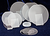
Description: InGaAs/InP Epitaxial Wafers With 'SuperLong' Wavelengths from 1.7µm - 2.6µMarktech Optoelectronics offers the highest purity InGaAs/InP Epitaxial Wafers in the industry today. Sophisticated manufacturing processes have been put in place to customize and produce high
-
Supplier: Rigaku Corporation
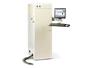
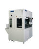
Description: Rigaku's WaferX 300 represents the culmination of 25 years of experience in the X-ray fluorescence analysis of thin films on silicon wafers. Specifically developed as an in-process metrology tool, the system incorporates "bridge tool" technology — servicing 6", 8", as well as the latest 12"
- Maximum Wafer / Part Size: 150.00000000000003 to 300.00000000000006 mm
- Measurements: Composition, Thickness - Film / Layer
- Mounting / Loading: Floor Mounted / Stand-alone
- Form Factor: Monitor / Instrument
-
Supplier: El-Cat, Inc.
Description: EL-CAT Inc. is a stocking distributor of Silicon Wafers, Compound Semiconductors and other Crystal Materials for use in electronics.
-
-
Supplier: Jiangyin Deli Laser Solutions Co., Ltd.
Description: Fast scribing speeds; high yield rates; high production capacity Produces high-quality results with no residue or melt-back Fully-automatic processing; integrated coating application, wafer cutting, and cleaning functions Laser type: DPSS 355nm ultraviolet laser Laser power: ≥5W Cooling
- Laser Output Power: 0 to 5 watts
- Type: Complete / Turnkey System
- Laser Operation: Laser Cutting
- Options / Components: Laser Head / Focusing Unit, Laser Optics / Beam Delivery, Laser System Enclosure, Monitoring Sensors / System
-
Supplier: Cosmic Equipment SpA
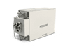
Description: The FTI-1000 is a purpose-built ATE system designed for high-coverage wafer-level testing of power discrete devices, wide-bandgap components, and gate-driver-integrated power ICs. Suitable for both engineering characterization and high-volume wafer sort, the system integrates
- Form Factor: Monitor / Instrument
- Applications: Semiconductor Wafers
-
Supplier: Cosmic Equipment SpA
Description: The FTI-1000 is a purpose-built ATE system designed for high-coverage wafer-level testing of power discrete devices, wide-bandgap components, and gate-driver-integrated power ICs. Suitable for both engineering characterization and high-volume wafer sort, the system integrates
- Form Factor: Monitor / Instrument
- Applications: Semiconductor Wafers
-
Supplier: Accuris
Description: Wafer Carriers for Use in Cleanrooms
-
Supplier: Cosmic Equipment SpA
Description: Wide bandgap SiC technology is opening up a whole new generation of high voltage power products for applications in transport, power transmission and green energy. M2 Wafer edition tests these upto 10kV on wafer before singulation, identifying defective product early and saving the
- Form Factor: Monitor / Instrument
- Applications: Semiconductor Wafers
-
Supplier: Cosmic Equipment SpA
Description: Wide bandgap SiC technology is opening up a whole new generation of high voltage power products for applications in transport, power transmission and green energy. M2 Wafer edition tests these upto 10kV on wafer before singulation, identifying defective product early and saving the
- Form Factor: Monitor / Instrument
- Applications: Semiconductor Wafers
-
Supplier: Park Systems, Inc.
Description: The XE-WAFER is a fully automated industrial AFM designed specifically to address surface roughness, trench width, depth, and angle measurements on 200mm & 300mm wafers in a production environment. The system provides superior accuracy and precision nanometrology over any other system
- Measurements: Critical Dimension / Trench Geometry, Defects / ADC, Roughness / Waviness
- Mounting / Loading: Floor Mounted / Stand-alone
- Form Factor: Monitor / Instrument
- Features: Non-contact, Non-destructive
-
Supplier: Fountyl Technologies Pte. Ltd.
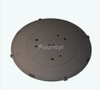
Description: point-like structure on the surface to provide better adsorption and stability. Prealigner chuck are widely used in semiconductor production equipment to absorb, fix, transfer and handle silicon wafers, wafers and various workpieces and materials.
- Materials: Ceramic
- Chuck Type: Electrostatic Chuck, Wafer Chuck
- Jaws: None / NA
- Features: Other / Specialty Chuck
-
Supplier: Newark, An Avnet Company
Description: WAFER ASSY FR/LK .100IN
-
Supplier: El-Cat, Inc.
Description: EL-CAT Inc. is a stocking distributor of Silicon Wafers, Compound Semiconductors and other Crystal Materials for use in electronics.
-
Supplier: El-Cat, Inc.
Description: EL-CAT Inc. is a stocking distributor of Silicon Wafers, Compound Semiconductors and other Crystal Materials for use in electronics.
-
Supplier: Hitachi High Technologies America, Inc.
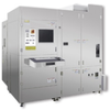
Description: The wafer surface inspection system LS series can detect defects on unpatterned wafers with a mirror-finished surface. Applied technology of laser scattering achieves high sensitivity and high throughput detection of small contaminants and various types of defects on wafer
- Mounting / Loading: Floor Mounted / Stand-alone
- Form Factor: Wafer Probing System
-
Supplier: El-Cat, Inc.
Description: EL-CAT Inc. is a stocking distributor of Silicon Wafers, Compound Semiconductors and other Crystal Materials for use in electronics.
-
Supplier: R. S. Hughes Company, Inc.
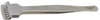
Description: The Excelta Three Star wafer tweezers is another quality product from Excelta. Offers a stainless steel wafer tip with a stainless steel body. Among all the other aspects of this product it offers the following resistant properties: anti-magnetic. The overall length measures 7 in.
- Tool Type: Tweezers
-
Supplier: Daitron Co., Ltd.
Description: The wafer edge grinders are designed to grind edge and circumference of a wide variety of wafers including silicon, compound semiconductors, such as, SiC, GaN, GaAs, and InP, oxide wafers, such as sapphire, quartz, LT, and LN, and glass, at high precision through
- Maximum Wafer / Part Size: 50.799972568014816 to 203.19989027205926 mm
- Mounting / Loading: Floor Mounted / Stand-alone
- Form Factor: Monitor / Instrument
- Applications: Semiconductor Wafers
-
Supplier: Accuris
Description: DETECTION OF OXIDATION INDUCED DEFECTS IN POLISHED SILICON WAFERS
-
Supplier: Nikon Metrology
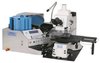
Description: The NWL200 series is the first lineup of wafer loaders for inspection microscopes capable of loading 100 micron thin wafers. Thanks to a new chuck system, the NWL200 series achieves highly reliable loading suitable for inspection of next-generation semiconductors. Improved
- Maximum Wafer / Part Size: 200 mm
- Measurements: Defects / ADC
- Mounting / Loading: Floor Mounted / Stand-alone
- Features: Non-contact, Non-destructive, Other
-
Supplier: Monocrystal, Inc.
Description: Wafers and blanks are produced from crystals grown using the Kyropoulos method. Advantages of our wafers: high material purity: > 99.997%; low impurity content Ti: < 1 ppm; low dislocation density: < 103 cm-2; orientation tolerance: up to ± 0.05 degrees. Sapphire wafers for
- Thickness / Wall Thickness: 0.005905515 to 0.0393701 inch
- Diameter: 2 to 10 inch
- Width / O.D.: 2 to 10 inch
- Features: Dielectric Ceramics / Materials
-
Supplier: Newark, An Avnet Company
Description: WAFER ASSY FR/LK .100IN 6 CKT
-
Supplier: Drytek Distribution
Description: Product Features: 300mm wafer size/ 200mm wafer size 300mm wafer cassette is made of PEEK material to prevent patricle generation Precise wafer access and reliable operation in equipment Identifiaction options: cardholders, RFID, bare code labels, laser marking.
-
Supplier: inTEST Thermal Solutions
Description: Temptronic ThermoChucks are conductive heating and cooling systems for wafer testing at temperature. Its primary use is for wafer testing in Probe Stations, as well as Laser Trim and Wafer Burn-in. A few specialized applications include Low leakage probing (fA level), and High
- Actuation: Electric
- Chuck Type: Wafer Chuck
-
Description: A ceramic wafer chuck is a specialized tool employed in the semiconductor industry to hold wafers in a secure position. It functions as a stable platform that guarantees consistent contact and precise positioning of the wafer during many procedures, including lithography,
- Features: Alumina / Aluminum Oxide, Specialty Ceramic
- Applications: Chemical / Materials Processing, Electrical / HV Parts
- Specialty Ceramic Type: Silicon Carbide, Silicon Nitride, Tungsten Carbide (WC)
- Shape / Form: Wafer Carrier / Holder
-
Supplier: R. S. Hughes Company, Inc.
Description: The Excelta Three Star wafer tweezers is another quality product from Excelta. Offers a stainless steel wafer tip with a stainless steel body. Among all the other aspects of this product it offers the following resistant properties: anti-magnetic. The overall length measures 7 in.
- Tool Type: Tweezers
-
Description: Examines the advantages of Embedded and FO-WLP technologies, potential application spaces, package structures available in the industry, process flows, and material challenges Embedded and fan-out wafer level packaging (FO-WLP) technologies have been developed across the industry over the
-
Supplier: ODG (Origin Data Global)
Description: 1x4P 4P 1 1mm 4 -25℃~+70℃ 1A Standing paste SMD,P=1mm Wire To Board Connector ROHS
-
Description: Innovacera standard aluminum nitride wafer diameters are from 50.8 mm (2 inch) to 200 mm (8 inch) ; mostly use are 6" aluminum nitride wafers and 8" AlN wafer substrates . AlN Wafers can be produced in various thicknesses from 0.125mm to 1mm with polished or lapped sides,
- Specialty Ceramic Type: Aluminum Nitride
- Features: Other, Specialty / Other, Specialty Ceramic
- Shape / Form: Wafer / Substrate
-
Supplier: MTI Instruments Inc.
Description: sori, site and global flatness. User-defined and ASTM/SEMI compliant scan patterns are used to generate full 3-dimensional (3D) wafer images. Customized data reports are available for viewing tabular data of each wafer measured with quick, easy export to your spreadsheet program.
- Maximum Wafer / Part Size: 300.00000000000006 mm
- Measurements: Area Mapping, Roughness / Waviness, Shape / Flatness, Thickness - Wafer / Disc (TTV)
- Technology: Capacitance / EM Gage
- Mounting / Loading: Manual Loading
-
Description: Ceramic wafer clamps are indispensible tools in semiconductor processing. They can be manufactured of high-purity alumina, zirconia, or silicon carbide, making them suited for high-temperature and corrosive environments.
- Features: Alumina / Aluminum Oxide, Specialty Ceramic
- Applications: Electrical / HV Parts
- Specialty Ceramic Type: Silicon Carbide, Tungsten Carbide (WC), Zirconia
- Shape / Form: Wafer Carrier / Holder
-
Supplier: MicroSense, LLC
Description: SECS/GEM communication. Automated calibration. Options Wafer prealigner HISCAN for Roughness and structures measurement Applications QA and QC of small size wafers, SiC, Sapphire, Glass, InP, etc…
- Maximum Wafer / Part Size: 50 to 100 mm
- Mounting / Loading: Manual Loading
- Form Factor: Monitor / Instrument
- Technology: Optical / Imaging System
-
Supplier: W.M. Berg
Description: Couplings Bellows Couplings Spider Couplings Absorbathane Couplings Oldham Couplings Universal Joint Couplings Wafer Spring and Disc Couplings Sleeve Couplings Neo-Flex Couplings Universal Lateral Couplings Flex-Thane Couplings Telescopic Universal Joint Couplings
- Bore Diameter: 0.3125 to 0.375 inch
- Coupling Diameter: 1.5 inch
- Coupling Length: 1.82 inch
- Angular Misalignment: 8 degrees
-
Supplier: R. S. Hughes Company, Inc.
Description: The Erem wafer tweezers is another quality product from Erem. Tip has a width of 1.181 in and thickness of 0.315 in. The overall length measures 5.906 in.
- Tool Type: Tweezers
-
Supplier: Broadcom Inc.
Description: The VMMK-3413 is a small and easy-to-use, broadband, directional detector operating in various frequency bands from 25 to 45 GHz with typical insertion loss of 0.8 dB. It is housed in the Avago Technologies' industry-leading and revolutionary sub-miniature WaferCap chip scale package (GaAsCap
- Input Frequency Range: 25,000 to 45,000 MHz
- Maximum DC Output Voltage: 674 millivolts
- Maximum DC Offset Output Voltage: 63 millivolts
- Package Type: Surface Mount Technology (SMT)











Find Suppliers by Category Top
More Information Top
 Indicates content that may require registration and/or purchase.

-
Plasma-assisted InP-to-Si low temperature wafer bonding
However, the increment in wafer-size has not fol- lowed the same progress and there are major concerns about the upscaling of InP wafer dimensions [43].
-
http://dspace.mit.edu/bitstream/handle/1721.1/76119/821059170-MIT.pdf?sequence=2
is again deposited on the backside of the InP wafer .
-
Low temperature InP layer transfer onto Si by helium implantation and direct wafer bonding
The SOG coated InP wafers were subsequently bonded to thermally oxidized Si(1 0 0) handle wafers and the bonded wafer pairs were annealed at 200 ◦ C for 20 h to achieve InP layer transfer onto Si(1 0 0) wafers …
-
Long-wavelength (1.55-μm) vertical-cavity lasers with InGaAsP/InP-GaAs/AlAs DBR's by wafer fusion
Before wafer fusion, the GaAs wafer was slightly etched with buffered HF, and the InP wafers were etched with H SO : H O : H O (3 : 1 : 1) solution and buffered HF to remove native oxides.
-
http://dspace.mit.edu/bitstream/handle/1721.1/62448/711100539-MIT.pdf?sequence=2
After removing the photoresist, the iron doped InP-InGaAsP- InP wafer was etched for 2 minutes in a C12 / SiCl4 /Ar ICP RIE etch chemistry to obtain a uniform 2pm etch depth across the sample.
-
Springer Handbook of Crystal Growth
As re- cently as 2006, a new application for high-speed laser modulation was developed using 6 in InP wafers bonded to silicon [7.1].
-
Lapping Technique of InP Single Crystal Wafer
Still no results related to InP wafer lapping technique have been reported, even though there are some papers about InP polishing process and mechanism [ADACHI,KURTH,WEI].
-
EMERGING OPTOELECTRONIC TECHNOLOGIES AND APPLICATIONS
When bulk InP wafers were patterned, the etch depth was approximately 500 nm.
-
http://dspace.mit.edu/bitstream/handle/1721.1/44718/297547620-MIT.pdf?sequence=2
3-10 Schematic showing a (100) InP wafer and the associated cleavage planes 81 .
-
http://dspace.mit.edu/openaccess-disseminate/1721.1/54241
The finished 150-mm-diameter InP wafer was then directly bonded to the SOI wafer and interconnected to the Si readout circuits by 3D vias.