Audio Power Amplifier Design Handbook, Fourth Edition
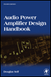
Figure 7.1 b shows a much less satisfactory method of compensation the addition of capacitance to ground from the VAS collector. This is usually called shunt or lag compensation, and as Peter Baxandall[2] aptly put it, 'The technique is in all respects sub-optimal'. We have already seen on page 104 that loading the VAS collector resistively to ground is a very poor option for reducing LF open-loop gain, and a similar argument shows that capacitative loading to ground for compensation purposes is an even worse idea. To reduce open-loop gain at 20 kHz to 50 dB as before, the shunt capacitor Clag must be 43.6 nF, which is a whole different order of things from 125 pF. The current in and out of Clag at 20 V rms, 20 kHz, is 155 mA peak, which is going to require some serious electronics to provide it. This important result is yielded by simple calculation, confirmed by Spice simulation. The input stage no longer constrains the slew-rate limits, which now depend entirely on the VAS.
A VAS working under these conditions will have poor linearity. The /c variations in the VAS, caused by the heavy extra loading, produce more distortion and there is no local NFB through a Miller capacitor to correct it. To make matters worse, the dominant pole P1 will probably need to be set to a lower frequency than for the Miller case, to maintain the same stability margins, as there is now no pole-splitting...