Mixed Analog-Digital Vlsi Devices and Technology
Filled with practical information, this reference book will help you grasp the nuances of mixed-signal VLSI-device models and layout that are crucial to the design of high-performance chips.
p-Well CMOS processes. The n-well CMOS process we have discussed above has its complement; this is shown in Fig. 5.27 and is referred to as a p-well process [ [1] [2] [3] [4] [5] [6]]. The substrate here is n type, and the individual wells are p type. This results in pMOS devices on a common substrate (which is tied to + V DD to prevent forward-biasing of pn junctions), and nMOS devices in p wells (one or more devices in each well). The nMOS devices end up having a larger body-effect coefficient, due to their higher body doping. The p-well process also provides, as by-products, npn bipolar transistors. The latter can typically have current gains of 100 and unity-gain frequencies on the order of 30 to 300 MHz.
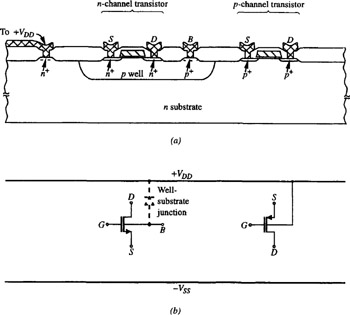
While both n-well and p-well processes have been used widely in the past, today n-well processes are dominant. In analog work, n-well processes are attractive because the pMOS devices (which can be advantageously used as input devices in amplifiers, due to their low noise) are inside wells, and thus their body does not have to be connected to a (usually noisy) power supply line; it can instead be tied to the transistor sources.