Handbook of Thin Film Deposition Processes and Techniques: Principles, Methods, Equipment and Applications, Second Edition
Krishna Seshan
Lithographically defined dimensions will continue to shrink as device scaling enables higher speeds and greater density of transistors. Lithography equipment, resist processes, and mask-making will change to meet the challenges. Gate oxides have to become thinner requiring changes in both growth and metrology equipment. As gate oxides become thinner, voltages must drop bringing about new material requirements. Lithography will call for highly planarized surfaces, causing higher demands on chemically-mechanically polished surfaces.
As transistor densities increase, the wiring levels providing interconnectivity will increase. This will increase the RC (resistance-capacitance) delay contribution of interconnections. The consequent drive to reduce resistance will drive the change from aluminum-based wiring metallurgy to copper-based metallurgy. In addition, the drive to decrease the dielectric constant will call for changes of the SiO 2-based dielectric to a class of "low-K" dielectrics.
Stringent demands will be made on contamination control, particle detection, and yield enhancement. One of the consequences will be the move from 8 inch to 12 inch wafers. This will drive consolidation of process steps.
These changing technologies will present new reliability challenges. This chapter discusses these trends and challenges.
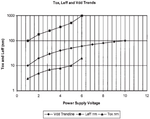
Gate oxide thickness, channel length, and power supply voltage scale along well-predicted trends as shown in Fig. 1. This figure is the basis for understanding the lithography challenges where line patterning in the range of 100 nm (0.1 m) and gate oxides of 30 nm (0.03 m) will need to be grown and measured.