
Products & Services
See also: Categories | Featured Products | Technical Articles | More Information-
Supplier: SemiProbe
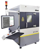
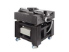
Description: SemiProbe IRIS inspection systems inspect, locate and identify defects created during wafer manufacturing, probing, bumping, dicing or general handling, providing microelectronic device manufacturers with accurate, timely quality assurance and process information. The IRIS
- Measurements: Area Mapping, Defects / ADC, Electrical Test - Parametric / In-line, Particle Contamination
- Mounting / Loading: Autoloading / In-line
- Technology: Optical / Imaging System
- Applications: Semiconductor Wafers
-
Supplier: Hitachi High Technologies America, Inc.
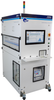
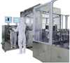
Description: The wafer surface inspection system LS series can detect defects on unpatterned wafers with a mirror-finished surface. Applied technology of laser scattering achieves high sensitivity and high throughput detection of small contaminants and various types of defects on
- Mounting / Loading: Floor Mounted / Stand-alone
- Form Factor: Wafer Probing System
-
Supplier: Nanotronics Imaging
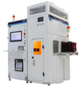
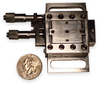
Description: requirements. Really, this is still all optics but we need to add some mechanics of focus and scanning. For this we manufacture our own precision translation stages and microscope stands. The nSpec® can be used with Nanotronics' nPlace™ wafer transfer system, an automatic robot
- Measurements: Defects / ADC
- Mounting / Loading: Manual Loading
- Technology: Optical / Imaging System
- Applications: Semiconductor Wafers
-
-
Supplier: Nikon Metrology
Description: The NWL200 series is the first lineup of wafer loaders for inspection microscopes capable of loading 100 micron thin wafers. Thanks to a new chuck system, the NWL200 series achieves highly reliable loading suitable for inspection of next-generation semiconductors.
- Maximum Wafer / Part Size: 200 mm
- Measurements: Defects / ADC
- Mounting / Loading: Floor Mounted / Stand-alone
- Features: Non-contact, Non-destructive, Other
-
Supplier: Hamamatsu Photonics Europe
Description: MiNY PL is an inspection system for micro LED wafers using the photoluminescence (PL) measurement method. MiNY is a registered trademark of Hamamatsu Photonics K.K. (China, EU, Japan, Taiwan, USA).
-
Supplier: Accuris
Description: STANDARD PRACTICE FOR CALIBRATING A SCANNING SURFACE INSPECTION SYSTEM USING MONODISPERSE POLYSTYRENE LATEX SPHERES DEPOSITED ON POLISHED OR EPITAXIAL WAFER SURFACES
-
Supplier: ASTM International
Description: wafers must be used as calibration wafers. The practice may also be extended to the calibration of SSISs intended to inspect other materials, such as gallium arsenide or other compound semiconducting compounds, in which case, clean, unpatterned, polished wafers of the type to be
-
Supplier: Daitron Co., Ltd.
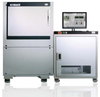
Description: The inspection and evaluation are automatically performed by placing devices on the stage and making the initial setting. The visual inspection machine is for the inspection of the top surface only, but we also offer the models for automatic inspection up to six sides.
- Mounting / Loading: Floor Mounted / Stand-alone
- Form Factor: Monitor / Instrument
- Technology: Optical / Imaging System
- Applications: Semiconductor Wafers
-
Supplier: Prior Scientific, Inc.
Description: begin analysis. The Prior Scientific motorized Shuttle Stage is designed to be used with the Nikon and Olympus wafer loader systems for 3, 4, 6, and 8 inch wafers. The system greatly reduces operator fatigue while increasing inspection accuracy and repeatability.
- Maximum X-Distance: 154 to 256 mm
- Maximum Y-Distance: 154 to 215 mm
- Minimum Step Size (Resolution): 0.04 µm
- Stage Type: Motorized Stage
-
Supplier: Park Systems, Inc.
Description: The XE-WAFER is a fully automated industrial AFM designed specifically to address surface roughness, trench width, depth, and angle measurements on 200mm & 300mm wafers in a production environment. The system provides superior accuracy and precision nanometrology over any other
- Measurements: Critical Dimension / Trench Geometry, Defects / ADC, Roughness / Waviness
- Mounting / Loading: Floor Mounted / Stand-alone
- Form Factor: Monitor / Instrument
- Features: Non-contact, Non-destructive
-
Supplier: ASTM International
Description: This standard was transferred to SEMI (www.semi.org) May 2003 1.1 This practice covers the determination of the accuracy with which a scanning surface inspection system (SSIS) reports the positions of localized light scatterers on a silicon wafer surface. Note 1-This practice
-
Supplier: Nikon Metrology
Description: XT V 160 NF Nanofocus X-ray inspection XT V 160 NF is a high-precision, flat-panel based X-ray inspection system that facilitates real-time imaging and defect analysis of next-generation wafer-level, semiconductor device and PCBA applications. Key benefits <0.1 µm feature
- Features: Computed Tomographic System
- Form Factor: Monitoring System
- Instrument Technology: Radiographic / X-ray
-
Supplier: Nikon Metrology
Description: series performs exceptionally precise optical inspection of wafers, photo masks, reticles and other substrates. 3 Models to Choose From L200: Offers 200mm wafer and mask inspection capabilities for reflected light illumination defect identification with various
- Total Magnification: 1 to 150 X
- Grade: Benchtop
- Remote Interface: Computer Interface, Image Analysis Processing Software
- Features: Digital Display, Fine Focus, Mechanical Stage
-
Supplier: TSI Incorporated
Description: This manually-loaded particle deposition system deposits PSL and SiO2 spheres as small as 20 nm. Calibrate and qualify your defect inspection tools with ease, confidence, and efficiency by producing high volumes of high-quality custom wafer calibration standards. Manual loading
- Maximum Wafer / Part Size: 150.00000000000003 to 300.00000000000006 mm
- Applications: CVD / PVD Films, Semiconductor Wafers
- Mounting / Loading: Manual Loading
- Features: Other
-
Supplier: TSI Incorporated
Description: This manually-loaded particle deposition system deposits PSL and SiO2 spheres as small as 10 nm. Calibrate and qualify your defect inspection tools with ease, confidence, and efficiency by producing high volumes of high-quality custom wafer calibration standards. Manual loading
- Maximum Wafer / Part Size: 150.00000000000003 to 300.00000000000006 mm
- Applications: CVD / PVD Films, Semiconductor Wafers
- Mounting / Loading: Manual Loading
- Features: Other
-
Supplier: TSI Incorporated
Description: This fully automated particle deposition system deposits PSL and SiO2 spheres as small as 20 nm. Calibrate and qualify your defect inspection tools with ease, confidence, and efficiency by producing high volumes of high-quality custom 300 mm and 200 mm calibration standards. Robotic
- Maximum Wafer / Part Size: 200 to 300.00000000000006 mm
- Applications: CVD / PVD Films, Semiconductor Wafers
- Mounting / Loading: Floor Mounted / Stand-alone
- Features: Other
-
Supplier: TSI Incorporated
Description: This fully automated particle deposition system deposits PSL and SiO2 spheres as small as 10 nm. Calibrate and qualify your defect inspection tools with ease, confidence, and efficiency by producing high volumes of high-quality custom 300 mm and 200 mm calibration standards. Robotic
- Maximum Wafer / Part Size: 200 to 300.00000000000006 mm
- Applications: CVD / PVD Films, Semiconductor Wafers
- Mounting / Loading: Floor Mounted / Stand-alone
- Features: Other
-
Supplier: SemiProbe
Description: Manual, semiautomatic and fully automatic systems with probing capabilities ranging from individual die to >450 mm wafers/substratesThe Probe System for Life (PS4L) family of wafer probing systems is designed based on SemiProbe™s patented adaptive architecture.
- Modules Included: Cameras or Imagers, Imaging & Analysis Software, Imaging Illuminators
- Image Source: Electron Microscope
- Applications: Electronics or Semiconductor Inspection
- System Type: Turnkey / Complete System
-
Supplier: Zygo Corporation
Description: substrate panels, ensuring that the system provides value for years to come. Customized chucks and sample holders are available to adapt the system for smaller panels or even singulated substrates to maximize application flexibility. And the system's integrated recipe-driven
- Maximum Wafer / Part Size: 650.0000000000001 mm
- Measurements: Area Mapping, Critical Dimension / Trench Geometry, Depth Profiling, Roughness / Waviness, Shape / Flatness
- Technology: Interferometer
- Mounting / Loading: Manual Loading
-
Supplier: Nikon Metrology
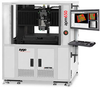
Description: Nikon's highest precision automated video measuring system is the “Master Reference Measuring System” for your metrology lab. Nikon's highest precision automated vision system, the NEXIV VMR-H3030, has the best specifications, accuracy and repeatability of any NEXIV measuring
- Applications: Electronics or Semiconductor Inspection
- Image Source: Optical Microscope
- System Type: Turnkey / Complete System
-
Supplier: Konica Minolta Sensing Americas, Inc.
Description: Now you can transfer the precision of laboratory measurements to production settings with this turnkey LED test system. This system is based on the proven CAS 140CT CCD Array Spectrometer, Keithley Series 2400/2600 Sourcemeter, and a control PC combined with tester software developed
- Features: Data Acquisition Capability
- Computer Platform: PC
- Applications: Spectrometry Test
-
Supplier: SemiProbe
Description: Manual Prober for contacting of active devices on both sides of the wafer. Precision controls enable the user to probe from the top side of the wafer, the bottom side of the wafer, or to simultaneously probe the top and bottom sides of the wafer.
- Modules Included: Cameras or Imagers, Imaging & Analysis Software, Imaging Illuminators
- Image Source: Electron Microscope
- Applications: Electronics or Semiconductor Inspection
- System Type: Turnkey / Complete System
-
Supplier: Newport MKS
Description: systems, as well as being an excellent choice for use in large substrate inspection and processing tools. The DynaQuiet™ option allows the system to operate at higher speed & acceleration (High Dynamic) without sacrificing stability at the point of interest or inducing
-
Supplier: JST Manufacturing, Inc.
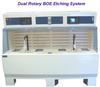
Description: Functions Data Logging Multiple Tank Processing 4" to 8" Wafer Capacity 360° Rotational Motion Dual Servo Motor Design Solvent & Acid Processing Models Options Bar Coding Color Panelview Remote PC Monitoring & Control GEM/SEC II Compliance 3rd. Party Electrical Inspection CE and Semi
-
Supplier: Evident Scientific
Description: Topside and backside macro inspections are also available for all wafer sizes Thin Wafer Inspection To meet the demands of thin wafer manufacturers, the new arm design of the AL120-LMB-90 model can handle a full cassette of 90 µm wafers. Serial Interface for
- Grade: Benchtop
- Eyepiece Style: Binocular
- Microscope Type: Compound
- Features: Digital Display, Mechanical Stage
-
Supplier: Integrated Sensing Systems, Inc.
Description: No Description Provided
- Capabilities: 2D / Surface Micromachining, 3D / Bulk Micromachining, Dielectric / CVD Thin Film, Dry Etching (Plasma / RIE), Inspection / Testing, Metallization - Electroplating, Metallization - PVD Thin Film, Oxidation / Doping, Packaging / Backend Processing, Photolithography, Screen Printing, Wafer Bonding,
- Materials: Compound Semiconductor, Glass, Quartz, SOI, Silicon
- Services: Design / Engineering, Pilot / Scale-Up, Production, Prototyping, R & D / Development
- Features: Midwest US Only, North America, Specialty / Other, United States Only
-
Supplier: Technic, Inc.
Description: System Overview The SEMCON 4000 is an automatic loading and unloading “wet bench” type wafer Under Bump Metalization tool, designed with processes for Nickel and Gold metalization of silicon and Ga/As wafers with aluminum or copper seed layer. The Semcon 4000 tool is designed
- Machinery Type: Automated System
- Process / Technology: Electroplating
- Application / Industry: Semiconductor / Wafer, Solar / Photovoltaic
-
Supplier: WDI Wise Device Inc.
Description: The LLC6 is a precise linear lens changer with 6 lens ports providing ultra fast, automatic lens changing without the need of re-qualifying the lens. It is the ideal tool for TFT-LCD and Photomask Inspection/Repair applications or other tasks where multiple optical magnifications are
- Features: Flat Panel Displays, In-situ / System Mounted, Non-contact, Non-destructive, Other
- Applications: Semiconductor Wafers
-
Supplier: Yamaha Corporation
Description: be used in the automotive industry for welding, painting, and assembly processes. It can also be used in the semiconductor industry for wafer transfer and inspection systems. The GF type linear actuator's excellent performance and reliability make it a versatile and valuable
- Stroke or X-Axis Travel: 98.42525 inch
- Rated Force: 198.45 lbs
-
Supplier: Newport MKS
Description: The HybrYXTM is a single plane XY hybrid air-bearing stage offers the advantages of a single plane air bearing stage at a much lower cost. HybrYX is well suited for semiconductor wafer inspection systems as well as being an excellent choice for use in large substrate (flat panel
- Stroke or X-Axis Travel: 13.779535 inch
- Y-Axis Travel: 25.590565 inch
-
Supplier: Park Systems, Inc.
Description: slope, and line width characterization. The completely automated XE-LCD is designed for characterization of flat panel displays as either an in-line or off-line inspection tool. • Automatic Non-Contact AFM measurement • Automatic navigation and focusing • Automatic glass handling • Automatic
- Measurements: Critical Dimension / Trench Geometry, Defects / ADC, Roughness / Waviness
- Mounting / Loading: Floor Mounted / Stand-alone
- Form Factor: Monitor / Instrument
- Features: Non-contact, Non-destructive
-
Supplier: Isotech, Inc.
Description: Wafer and mask positioning Inspection systems
-
Supplier: PI (Physik Instrumente) L.P.
Description: encoders supply explicit position information that enables immediate determination of the position. This means that referencing is not required during switch-on, which increases efficiency and safety during operation. Application fields Tomography, beamline systems, wafer metrology,
-
Supplier: Park Systems, Inc.
Description: Hard Disk Drive (HDD) manufacturers can now reliably depend on Park Systems’ XE-PTR, a fully automated industrial in-line AFM for automatic Pole Tip Recession measurements on rowbar-level sliders. As most HDD manufacturers are turning to PMR (Perpendicular Magnetic Recording), sub-nano scale
- Features: Data Storage / Memory, Non-contact, Non-destructive
- Measurements: Defects / ADC
- Mounting / Loading: Floor Mounted / Stand-alone
- Form Factor: Monitor / Instrument
-
Supplier: PI (Physik Instrumente) L.P.
Description: encoders supply explicit position information that enables immediate determination of the position. This means that referencing is not required during switch-on, which increases efficiency and safety during operation. Application fields Tomography, beamline systems, wafer metrology,
- Load Capacity: 42.712 to 173.096 lbs
- Shape: Flat, Round
- Design: Metric












Find Suppliers by Category Top
Featured Products Top
-

-
INSACO Offers Wafer Carriers With or Without Multiple Holes INSACO, Inc has become recognized as a worldwide leader in custom machined ceramic and sapphire parts for the semiconductor industry. Through this experience (read more)
Browse Glass Fabrication Services Datasheets for Insaco, Inc. -
Watch>> - Sapphire for GaAs, Indium Phosphide, & Other Semiconductors Sapphire Wafer Carriers (read more)
Browse Wafer Cassettes Datasheets for Insaco, Inc. -
Positioning Solutions Efficient wafer inspection and metrology are essential in semiconductor manufacturing to prevent yield loss. Achieving this requires precise wafer positioning, which enables fast and reliable analysis of defects and particles at every production stage. PI’s cutting (read more)
Browse Linear Slides and Linear Stages Datasheets for PI (Physik Instrumente) L.P. -
Wafer Manufacturing: Wafer stages for photolithography systems, etching chucks, electrostatic chucks for ion implantation equipment, and thin-film deposition systems (read more)
Browse Wafer Chucks Datasheets for Fountyl Technologies Pte. Ltd. -
Watch>> - Sapphire for GaAs, Indium Phosphide, & Other Semiconductors Sapphire Wafer Carriers (read more)
Browse Wafer Cassettes Datasheets for Insaco, Inc. -
and Wafer Inspection Systems (read more)
Browse Wafer Chucks Datasheets for Fountyl Technologies Pte. Ltd. -
offers high thermal stability, chemical resistance, and long-term performance under demanding manufacturing conditions. It is suitable for wafer transfer systems, inspection equipment, semiconductor processing tools, and other precision automation (read more)
Browse Wafer Chucks Datasheets for Fountyl Technologies Pte. Ltd. -
. Applications: Perfect for wafer clamping in exposure devices, inspection tools, and transportation systems in semiconductor production, ensuring precision and reliability in critical processes. Engineers (read more)
Browse Wafer Chucks Datasheets for Fountyl Technologies Pte. Ltd. -
in wafer dicing, grinding, thin-film deposition, and automated optical inspection (AOI (read more)
Browse Wafer Chucks Datasheets for Fountyl Technologies Pte. Ltd.
Conduct Research Top
-
Circuit Pattern Inspection on Wafer Samples
When microscopic observation of both the circuit pattern and color of a wafer sample is required, the conventional method calls for darkfield illumination for the former and brightfield illumination for the latter, with repeated switching between the two techniques. This method of observation
-
SmartMore Efficient Vision Inspection System for Silicon Wafer
Chipsets are typically designed to work with a specific series of microprocessors because it regulates the communication between the processor and the external devices. It plays a vital role in determining system performance. In the chip production process, wafer bumps critical chip components need
-
EETimes.com | Electronics Industry News for EEs & Engineering Managers
software with IA-64 patents NEW YORK -- A flurry of more than 20 new patents suggests Intel Corp. is expanding its time-tested legal strategy to prevent cloning of its new, flagship IA-64 architecture. ADE claims KLA-Tencor violating wafer inspection patent WESTWOOD, Mass. -- ADE Corp. here has
-
EETimes.com | Electronics Industry News for EEs & Engineering Managers
: Micron cell innovation changes DRAM economics National's Q2 sales jumps 11%, sees 0-3% growth in Q3 The price plunge peters out Xilinx co-founder, executive Bernie Vonderschmitt dies ICOS acquires Siemens' wafer inspection business Intel mulling chip plant
-
EETimes.com | Electronics Industry News for EEs & Engineering Managers
and South Korea this week, following moves initiated last year in U.S. courts and with the U.S. International Trade Commission. France's i2S rolls out module for wafer inspection
-
EETimes.com | Electronics Industry News for EEs & Engineering Managers
, the worldwide chip-equipment industry posted a book-to-bill ratio of 0.82 in April, up from 0.71 in March, according to VLSI Research Inc. Applied to roll 'bright field' inspection tool, says report Applied Materials Inc. is expected to introduce "a bright field wafer inspection tool. " The Week
-
An Innovative Cabling Concept Improves Reliability for Multi-Axis Stage Systems
up to 4 separate cables (with diameters of 8 to 14 mm). And up to 27 electrical wires must be connected. Wafer inspection systems in the semiconductor industry typically consist of a stack of XYZ linear stages plus a theta rotary unit. So there can easily be perhaps 16 connectors at the final
-
EETimes.com | Electronics Industry News for EEs & Engineering Managers
drives MicroSensors receives patent for silicon micromachined gyro sensor France's Soitec, Gemplus target SOI wafers for smart-card ICs Veeco adds thin-film inspection, ion-beam deposition through two mergers PMC-Sierra's networking-chip strategy lifts earnings Patton leaves Schlumberger
More Information Top
 Indicates content that may require registration and/or purchase.

-
Wafer Inspection / Inspection Systems
I-5320 / I-6300 - Electron Beam Wafer Inspection System .
-
The P300: A system for automatic patterned wafer inspection
Dora et al.: P300---Automatic Wafer Inspection System .
-
Wafer Pattern Defect Detection: An Automatic Inspection Technique
The performance and efficiency of such an automatic wafer inspection system will un- doubtedly lead to its replacing the current conventional method of manual microscopic exam- ination by the human eye in the near future.
-
The P300: An Approach to Automated Inspection of Patterned Wafers
As IC groundrules shrink, manual optical inspection of multilevel patterned wafers becomes ineffective if not impossible, and efforts to develop automatic wafer inspection systems have expanded.
-
Evaluation of the yield impact of epitaxial defects on advanced semiconductor technologies
As shown in Figure 6, the inspection capture rate for particles was nearly 100 percent versus other product wafer inspection systems (e.g., AIT-X and KLA 213X).
-
Automated Detection of Wafer Surface Defects by Laser Scanning
Applica- tions of these wafer inspection systems in process control and incoming inspection are described.
-
Wafer Inspection / KLA-Tencor Corp.
Candela CS20 - High Brightness LED Automated Wafer Inspection System .
-
Wafer Inspection Technology For Submicron Devices
There are applications of wafer inspection systems which fit into the process improvement cycle.