
Products & Services
See also: Categories | Featured Products | Technical Articles | More Information-
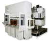
Supplier: JST Manufacturing, Inc.
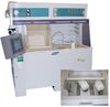
Description: JST's Single Wafer Etching and Stripping System utilizes an automated chemical spray process on a single wafer. The system includes oscillating spray nozzles, adjustable wafer speed (RPM) and precision adjustment of the distance between the nozzles and the surface of the wafer. It's automated
-
Supplier: JST Manufacturing, Inc.
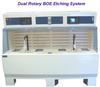
Description: JST offers affordable semi-automated systems in both rotary and linear transfer designs. Rotary Transfer stations can accomodate single or dual rotary arms. JST's robot uses DC servo motors for efficient transfers with high reliability. This servomotor technology provides precise position
-
Supplier: Technic, Inc.
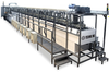
Description: Vertical processing is widely acknowledged as the preferred method for achieving optimum side-to-side and edge-to-edge uniformity. Technic’s MP200CS is an advanced roll-to-roll wet processing system that offers a variety of key benefits for today’s flexible printed circuits, metal foils, and
-
-
Supplier: Technic, Inc.
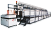
Description: Technic has long been pioneer in the ongoing development of printed circuit board wet processing equipment and chemistry. Our ongoing commitment to application research and in-house product development has enabled us to continuously offer our customers the most advanced technology available
- Machinery Type: Continuous Web - Reel to Reel
- Process / Technology: Electroplating
- Application / Industry: Printed Circuit Boards (PCB)
-
Supplier: Hitachi High Technologies America, Inc.
Description: Conductor Etch System M-8000 Series is utilized for hard mask and silicon etching for 32nm and beyond. Hitachi High-Tech developed new process flows, such as double patterning and new material etch processes such as high-k dielectric/metal gate through JDP (Joint Development Program) with
- Applications: Etching - Plasma / Wet
- Mounting / Loading: Floor Mounted / Stand-alone
-
Supplier: Hitachi High Technologies America, Inc.
Description: Plasma) etch system provides superior performance in profile control as well as in higher etching rate and selectivity compared to conventional ion-milling processes. Applicable wafer diameter 150mm, 200mm
- Applications: Etching - Plasma / Wet
- Mounting / Loading: Floor Mounted / Stand-alone
-
Supplier: Hitachi High Technologies America, Inc.
Description: Next generation memories such as FeRAM (Ferroelectric Random Access Memory), ReRAM (Resistance Random Access Memory) and MRAM (Magnetoresistive Random Access Memory) require etching of novel non-volatile materials. However, by-product adhesion inside of etch chamber causes significant
- Applications: Etching - Plasma / Wet
- Mounting / Loading: Floor Mounted / Stand-alone
-
Supplier: Terra Universal, Inc.
Description: Terra’s comprehensive range of constant-temperature baths, etching baths, dump risers, and other processing equipment is ideally suited for the high-purity requirements of the semiconductor industry. Microprocessor controls ensure the integrity of your operations.
-
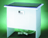
Supplier: Terra Universal, Inc.
Description: Ideal for etching, stripping and cleaning Ultra-pure, 99.995% contaminant-free processing vessel is ideal for critical chemistries Externally bonded 5-sided circuit heating element provides efficient, even heating for improved process yields Redundant safety features minimize potential damage
-
Supplier: HORIBA Instruments, Inc.
Description: The CS-137 is a high-precision chemical solution concentration monitor designed to meet the strict demands of semiconductor wet-etching processes. Etching processes use BHF solution to etch silicon oxide and remove particles from the wafer surface. The CS-137 continually
-
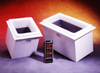
Supplier: Terra Universal, Inc.
Description: Ideal for etching, stripping and cleaning Seamless quartz vessel is 99.995% contaminant-free Externally bonded 5-sided circuit heating element provides efficient, even heating for improved process yields Redundant safety features minimize potential damage caused by runaway temperatures PVDF
-
Supplier: Terra Universal, Inc.
Description: Precisely controlled low- or high-temperature processing (when used with RCe recirculating module) Natural polypropylene tank is ideal for etching, stripping, and developing with HF, KOH, CrO, and other chemistries (PVDF also available) Also functions as a stand-alone ambient-temperature bath
-
Supplier: AirClean Systems
Description: AirClean® Systems’ wet scrubber system is a wet contact scrubber that is suitable for water soluble gases. Each scrubber is constructed from thermoplastics that are resistant to the gases being scrubbed. Scrubber Features: Direct mounting to fume hood exhaust eliminates contaminated
- Pollutants Scrubbed: Acid
- Orientation: Vertical
- Process Type: Wet
-
Supplier: Schmalz Inc.
Description: Wafer gripper for extreme fast, reliable, precise and gentle handling of wet wafers in wet bench applications Handling of wafers after etching and cleaning processes Loading and unloading of conveyor belts Fully or partially automated production of silicon wafers with maximum
-
Supplier: Schmalz Inc.
Description: Wafer gripper for extreme fast, reliable, precise and gentle handling of wet wafers in wet bench applications Handling of wafers after etching and cleaning processes Loading and unloading of conveyor belts Fully or partially automated production of silicon wafers with maximum
-
Supplier: Kayaku Advanced Materials, Inc.
Description: Low viscosity, solvent-free photo-curable NIL resist specifically designed for use with rigid and gas-impermeable working stamps like COC, COP, OrmoStamp®, or glass. Mask for pattern transfer processes (dry and wet etching) No adhesion promoter or primer necessary Very low release
- Applications: Electronics / Microelectronics
- Thick Film Type: Resistor
-
Supplier: Hiden Analytical
Description: The Hiden Plasma Workstation, an integrated RF-ICP reactor / plasma analyser system for all you plasma process studies.
- Form Factor: Controller, Monitor / Instrument
- Measurements: Deposition Rate
- Applications: Etching - Plasma / Wet, Optical Components
- Mounting / Loading: In-situ / System Mounted
-
Supplier: Hiden Analytical
Description: The ESPion advanced Langmuir probe for rapid, reliable and accurate plasma diagnostics for industry and academia.
- Form Factor: Controller, Wafer Probing System
- Measurements: Deposition Rate
- Applications: Etching - Plasma / Wet
- Mounting / Loading: In-situ / System Mounted
-
Supplier: ASTM International
Description: alloys. For aluminum alloys: vapor or non-etching alkaline degreasing; sulfuric acid-sodium dichromate or sulfuric acid-ferric sulfate solution etching; phosphoric and sulfuric acid anodizing; propriety cleaning; secondary bonding; brush plate bond etching; mechanical abrasion;
-
Supplier: Hiden Analytical
Description: The Hiden EQP is a combined Mass / Energy analyser for the analysis of positive AND negative ions, neutrals, and radicals from plasma processes.
- Form Factor: Controller, Monitor / Instrument
- Measurements: Deposition Rate, Endpoint Detection / Plasma Diagnostics
- Applications: Etching - Plasma / Wet, Optical Components
- Mounting / Loading: In-situ / System Mounted
-
Supplier: Tronics Microsystems
Description: Tronics will take on your MEMS project and bring it to production, whether it is a mature product or still a concept requiring prototyping iterations. Our goal is to establish reliable supply chains for your MEMS products. We have strong experience of industrializing complex MEMS with sensitive
- Services: Design / Engineering, Production, Prototyping, R & D / Development
- Capabilities: Dry Etching (Plasma / RIE), Inspection / Testing, Metallization - Electroplating, Oxidation / Doping, Packaging / Backend Processing, Photolithography, Screen Printing, Wafer Bonding, Wet / Chemical Etching
- Features: Europe Only, Specialty / Other
- Materials: Quartz, SOI, Silicon
-
Supplier: PSI Extrusions
Description: chromate finish (Mil-C-5541) Etching Satin (Type II) Off-Site Finishing Services Bright Dip Wet Painting Film coating
- Materials: Aluminum
- Coating Capabilities: Chemical Finish / Conversion, Painting, Powder Coating, Screen Printing / Selective Coating
- Industry Served: Commercial / Professional, OEM / Industrial
- Functions & Features: Conductive, Corrosion / Rust Preventive
-
Supplier: Integrated Sensing Systems, Inc.
Description: No Description Provided
- Capabilities: 2D / Surface Micromachining, 3D / Bulk Micromachining, Dielectric / CVD Thin Film, Dry Etching (Plasma / RIE), Inspection / Testing, Metallization - Electroplating, Metallization - PVD Thin Film, Oxidation / Doping, Packaging / Backend Processing, Photolithography, Screen Printing, Wafer Bonding,
- Materials: Compound Semiconductor, Glass, Quartz, SOI, Silicon
- Services: Design / Engineering, Pilot / Scale-Up, Production, Prototyping, R & D / Development
- Features: Midwest US Only, North America, Specialty / Other, United States Only
-
Supplier: Universal Semiconductor, Inc.
Description: No Description Provided
- Capabilities: 2D / Surface Micromachining, 3D / Bulk Micromachining, Dielectric / CVD Thin Film, Dry Etching (Plasma / RIE), Inspection / Testing, LIGA, Metallization - Electroplating, Metallization - PVD Thin Film, Oxidation / Doping, Packaging / Backend Processing, Photolithography, Wafer Bonding, Wet /
- Materials: Ceramic, Compound Semiconductor, Glass, Metal / Nickel, Polymer / Organic, Quartz, SOI, Silicon
- Services: Design / Engineering, Pilot / Scale-Up, Production, Prototyping, R & D / Development
- Features: North America, Southwest US Only, Specialty / Other, United States Only
-
Supplier: Process Sensing Technologies USA
Description: its measurements is guaranteed. Features: Precision measurement from 0.1 to 2000ppmV Fast response in both dry to wet and wet to dry transitions Simple, low cost, on-site maintenance with long service intervals Dryer can be replaced by the user in 10 minutes Accuracy of 0.1ppmV or 10%
- Instrument Type: Analyzer
- Features: Self Calibration
- Measurement Type: Trace
-
Supplier: Plansee SE
Description: Mo/Cu wet etching. In electrode layers, copper is mostly used in combination with a molybdenum adhesion promotion layer/diffusion barrier. To structure the Mo-Cu multilayers, we have worked together with the Korean Aerospace University and leading chemicals manufacturers to develop a
- Type: Sputtering Target
-
Supplier: HORIBA Instruments, Inc.
Description: The CS-153 is a high-precision chemical solution concentration monitor designed to meet the strict demands of semiconductor wet-etching processes. Etching processes use FPM solution to etch silicon oxide and remove particles from the wafer surface. The CS-153 continually
- Process Media Temperature: 68 to 176 F
- Operating Temperature: 68 to 77 F
- Electrical Output: Analog Current Output, Switch / Alarm Relay Output
- Display Type: Digital Display
-
Supplier: HORIBA Instruments, Inc.
Description: The CS-153N is a high-precision chemical solution concentration monitor designed to meet the strict demands of semiconductor wet-etching processes. Etching processes use HF/HNO3 solution to etch silicon oxide and remove particles from the wafer surface. The CS-153N continually
- Process Media Temperature: 68 to 176 F
- Operating Temperature: 68 to 77 F
- Electrical Output: Analog Current Output, Switch / Alarm Relay Output
- Display Type: Digital Display
-
Supplier: ASTM International
Description: by coils. While the material is properly magnetized, the magnetic particles may be applied by either the dry method, wet method, or fluorescent method. The parts shall also be sufficiently demagnetized after inspection so that residual or leakage fields will not interfere with future
-
Supplier: ASTM International
Description: to characterization of stainless steel surfaces that are smoother than R a = 0.25 μm, as determined by a contact-stylus profilometer and defined by ANSI B46.1. The magnifications and height scales used in this test method were chosen with this smoothness in mind. 1.2.2 Intentional etching or
-
Supplier: Boyd
Description: hairline, auto degreasing or cleaning, laser etching for precise finishing needs Cleanroom manufacturing Class 100 to Class 100K, ultrasonic cleaning Levelling with CMM (Coordinate Measuring Machine) Complete assembly solutions including rivets, studs, brackets, NC riveting, auto tapping
- Secondary Operations: CNC Machining, Drilling / Tapping, Heat Treating / Stress Relieving, Painting / Powder Coating, Tool Making, Welding
- Features: East Asia / Pacific Only, Europe Only, North America, Oceania Only, Other
- Materials: Ferrous Metals, Nonferrous Metals
- Stamping Capabilities: Progressive Dies
-
Supplier: ASTM International
Description: to characterization of stainless steel surfaces that are smoother than Ra = 0.25 μm, as determined by a contact-stylus profilometer and defined by ANSI B46.1. The magnifications and height scales used in this test method were chosen with this smoothness in mind. 1.2.2 Intentional etching or
-
Supplier: Shenzhen Jewellok Technology Co., Ltd.
Description: material science. By using 316L electropolished stainless steel with a 5Ra surface finish, the equipment prevents corrosion and “shedding,” ensuring the chemical remains as pure at the point of use as it was at the source. This is critical for processes like Wet Etching and Chemical
- Body Material: Stainless Steel
-
Supplier: Shenzhen Jewellok Technology Co., Ltd.
Description: pressure regulators, the CDS prevents “shedding”—the release of metal ions or particles into the chemical stream. This is vital for sub-micron fabrication, where even a single contaminant can lead to catastrophic yield loss during wet etching or CMP processes. Safety is equally
- Body Material: Stainless Steel
-
Supplier: Shenzhen Jewellok Technology Co., Ltd.
Description: ability to perform precise blending and dilution automatically. In processes like Chemical Mechanical Planarization (CMP) or wet etching, chemicals often require exact mixing ratios to be effective. By utilizing PLC automation and non-contact sensors, the CDM eliminates human error,
- Body Material: Stainless Steel














Find Suppliers by Category Top
Featured Products Top
-
 characteristics of multi-cartridge filter housings and their specific applications in semiconductor liquid filtration. Specific Applications in Semiconductor Liquid Filtration1. Wet Etching and (read more)
Browse Filter Housings Datasheets for Harbory Filtration -
particle contamination. Its low erosion rate reduces process tool cost of ownership. Perlast G65HP is ideal for use in wet and dry semiconductor processes including: Plasma Etching Ash/Resist Stripping LPCVD, HDPCVD, PECVD, SACVD, ALD Cleaning PVD Perlast G65HP can be molded into O-rings, seals, NW/KF fittings and custom components to suit any application. (read more)
Browse Rubber and Elastomer Molding Services Datasheets for Precision Polymer Engineering Ltd. -
than 100 μm film thickness in a single coat Aqueous developer compatible (TMAH & KOH) Wet stripping in conventional strippers Excellent dry etch resistance Material Uses: (read more)
Browse Thick Film Materials Datasheets for Kayaku Advanced Materials, Inc. -
. Applications: Semiconductors: Ideal for printed circuit boards, etching baths, wet processing equipment, and ultrapure water filtration. Oil & Gas: Offers comprehensive filtration solutions for upstream (read more)
Browse Filter Housings Datasheets for Harbory Filtration -
resistance to aggressive oxygen, chlorine and fluorine-based plasmas. Together with outstanding thermal and mechanical resistance qualities and similarly low particle generation to Perlast® G65HP, Perlast® G67G is ideally suited to wet and dry etching, stripping, cleaning and PVD processes. (read more)
Browse O-rings Datasheets for Precision Polymer Engineering Ltd. -
are key to reducing process contamination, significantly increasing yield and reducing operational downtime. Perlast® Helios G7HA has been developed for use in wet and dry semiconductor processes, including etching, stripping and cleaning. The new material is expected to be moulded into (read more)
Browse O-rings Datasheets for Precision Polymer Engineering Ltd. -
products, and finished products. Food and Beverage : Used to filter beverages, oils, and other food products to remove impurities and improve their quality. Electronic industry liquid crystal wet process : filter etching solutions, removing impurities (read more)
Browse Filter Elements Datasheets for Harbory Filtration -
CYTOP™ transparent amorphous fluoropolymers don’t require a baking process for adhesion and imparts a protective coating against acid or alkaline etching as well as insulation properties to semiconductor and MEMS-related materials. Transparent amorphous fluoropolymers can be (read more)
Browse Polymers and Plastic Resins Datasheets for AGC Chemicals Americas, Inc.
Conduct Research Top
-
MSilica Nanoparticles Treated by Cold Atmospheric-Pressure Plasmas Improve the Dielectric Performance of Organic-Inorganic Nanocomposites
to the. stamping process [46], was removed by 5 min of wet etching. using TMAH 25% at 701C. To facilitate the stamping. Figure 1. 2-D top. view schematic. of the microdevices. All dimensions. are in mm. Figure 2. log(g) surface plot of (A) device 1, (B) device 2, (C). device 3, (D) device 4, at an applied
-
Fabrication of GaAs Devices
Fabrication of GaAs Devices. Focusing on all aspects of GaAs processing that deal with GaAs free surfaces and interfaces between GaAs and metal contacts or dielectrics, this detailed text offers pragmatic advice on cleaning and passivation, wet and dry etching and photolithography.
More Information Top
 Indicates content that may require registration and/or purchase.

-
MEMS Materials and Processes Handbook
Complementing the coverage of dry etching, wet etching processes for MEMS micromachining are covered in Chapter 8 with a comprehensive recipe and reference list included in this chapter to aid in finding etch rates and etch selectivities for a wide range of …
-
Introduction to Microfabrication 2nd Edition
Etching, Wet Etching , Plasma Etching (RIE), .
-
Encyclopedia of Microfluidics and Nanofluidics
Different etchants used in anisotropic wet etching have specific etch rates for each crystallographic plane in the material being removed.
-
MEMS/NEMS
Wet etching processes can be made selective by doping the silicon heavily with boron creating what is called a p+ etch stop.
-
Fabrication of GaAs Devices
4 Wet etching and photolithography of GaAs and related alloys 117 .
-
Encyclopedia of Microfluidics and Nanofluidics
Different etchants used in anisotropic wet etching have specific etch rates for each crystal- lographic plane in the material being removed.
-
Introduction to Semiconductor Manufacturing Technology
Wet Etch Process ..............................................................................................
-
Handbook for Cleaning for Semiconductor Manufacturing: Fundamentals and Applications Complete Document
The Chemistry of Wet Etching .
-
Bonding in Microsystem Technology
Fast wet etching ..........................................................
-
Handbook of Porous Silicon
Micromachining and wet etching Etching (wet .