Depending upon the physical arrangement of the wire channels of data links, electrical signaling schemes for data transmission over wire channels can be classified into single-ended, fully differential, pseudo-differential, and incremental signaling schemes. They can also be categorized into voltage-mode and current-mode signaling schemes on the basis of the signal carriers of data links. This chapter examines the advantages and limitations of these signaling schemes. Section 4.1 compares the characteristics of voltage-mode and current-mode signaling. In Section 4.2, various voltage-mode signaling schemes, namely single-ended signaling, fully differential signaling, pseudo-differential signaling, and voltage-mode incremental signaling schemes are investigated and their pros and cons are examined in detail. Section 4.3 focuses on unipolar and bipolar current-mode signaling, and current-mode incremental signaling schemes. The chapter is summarized in Section 4.4.
4.1 Voltage-Mode Signaling Versus Current-Mode Signaling - A Comparison
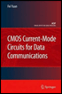
Shown in Fig.4.1 is a typical voltage-mode circuit. The signal conveyed to the channel by the driver is the output voltage of the inverter. It is determined from
| (4.1) | 
|
where R n and R p are the channel resistance of the nMOS and pMOS transistors in the triode, respectively, C L is the load capacitance of the driver, V OL and V OH are the voltage of Logic-0 and Logic-1 states, respectively, C LV OL ?( t) and C LV OH ?( t) quantify the effect of the initial voltage of the load capacitor at the onset of charging and discharging processes, respectively.
Copyright Springer Science+Business Media, LLC 2007 under license agreement with Books24x7