Digital Circuit Analysis and Design with Simulink Modeling and Introduction to CPLDs and FPGAs, Second Edition

For all exercises, assume that the variables are available in the uncomplemented form only.
| 1. | Implement the theorem A+ A=1 using
|
|
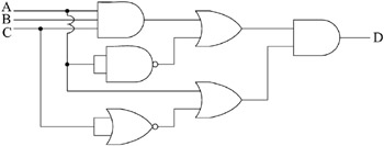
| 2. | For the logic diagram below, derive the Boolean expression and simplify it if possible. Then, implement the logic diagram for the simplified expression.  |
|
| 3. | Use a single SN74LS00 Quad 2-input NAND gate IC device to implement the Boolean expression |
|
| 4. | Use NAND gates only to implement the Boolean expression W=X Y+Y Z+ XZ. |
|
| 5. | For this exercise assume that logical 0=0 volts=Low, logical 1=5 volts=High, and the inputs to AND, NAND, OR, NOR, XOR, and XNOR gates are A=11000101 and B=10110010 during the time interval T 1 ?T ?T 2. Sketch the timing diagrams for AB , AB , A+B, A+B, A ?B, and A ? B for this time interval |
|
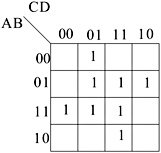
| 6. | A Boolean expression is mapped in the K-map shown below. Derive the simplest Boolean expression in terms of the variables A, B, C, and D.  |
|
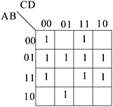
| 7. | A Boolean expression is mapped in the K-map shown below. Derive the simplest Boolean expression in terms of the variables A, B, C, and D.  For Exercises 8 through 14, derive the truth tables and by the use of K-maps derive the simplest Boolean expressions for the output(s). There is no need to draw the logic diagrams. |
|
| 8. | Design... |
