Electronics Manufacturing: With Lead-Free, Halogen-Free, and Conductive-Adhesive Materials

This chapter gives a brief overview of packaging technologies, trends in electronics packages, and conductive adhesive technology, and also introduces the scope and nature of the following chapters. The intent is to provide a fundamental understanding of ECA technology and to develop high-performance conductive adhesives for solder replacement. This chapter also includes a detailed outline of the research goals and selected approaches to gaining a fundamental understanding and developing solder replacement conductive adhesives.
Packaging of electronic circuits is the science and art of establishing interconnection and a suitable operating environment for predominantly electrical circuits to process or store information.1 Packaging has four main functions:
Signal distribution, involving mainly topological and electromagnetic considerations
Power distribution, involving electromagnetic, structural, and materials aspects
Heat dissipation (cooling), involving structural and materials considerations
Protection (mechanical, chemical, and electromagnetic) of components and interconnections
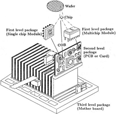
Levels of electronic packaging are defined in Fig. 17.1. In first-level packaging, the integrated circuit is assembled into a package such as a quad flat pack, pin grid array, or ball grid array using wiring bonding, tape automated bonding, or flip chip bumping assembly techniques. The packaged device is then attached either directly to a printed circuit board or to another type of substrate, which is defined as second-level packaging. The next level of packaging (third or higher) may be the outer shell of a small piece of equipment.
The packaging concepts and technologies in all packaging levels are undergoing...