Frequency-Domain Characterization of Power Distribution Networks
Chapter 3: Characterization and Modeling of Vias

3.1 Introduction

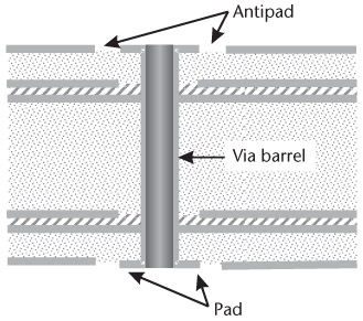
Vias form part of the path in PDN carrying the current from source to load. They stitch common planes together vertically and can also provide a current return path for signals. A via consists of a barrel, pad, and antipad. The barrel is a conductive cylinder that allows electrical connection between PCB or package layers. The pad is used to connect the via barrel to a signal or supply trace. Nonfunctional pads can also exist on layers where no trace connection is made. Antipads are clearance holes between the pad and the surrounding plane. The most common type of via, called a through via, extends from the top of the stackup to the bottom layer. For PCBs, through vias are formed by drilling a hole through the PCB and plating it with copper. This plating forms the wall of the via barrel, which are typically hollow. A via constructed in this manner is illustrated in Figure 3.1 and called a plated-through-hole (PTH) via.


Figure 3.1: Illustration of a PTH via cross-section connecting to two plane layers.

3.2 Via Partial Inductance

The inductance, not the capacitance, of vias is usually the primary concern in PDN applications because it increases the impedance between the source and load. Consequently, it is very useful to have expressions to calculate the inductance of a via. In this section, a complete derivation of via inductance from energy relations is presented, outlining all the key steps and assumptions [1]. Based on this derivation, the concept...

UNLIMITED FREE
ACCESS
TO THE WORLD'S BEST IDEAS

SUBMIT
Already a GlobalSpec user? Log in.

This is embarrasing...

An error occurred while processing the form. Please try again in a few minutes.

Customize Your GlobalSpec Experience

Category: AC Power Connectors
Finish!
Privacy Policy

This is embarrasing...

An error occurred while processing the form. Please try again in a few minutes.