IC Layout Basics: A Practical Guide

This book teaches the basics of IC (Integrated Circuit) layout in jargon-free, plain-English, understandable to those without an EE degree.
In our first two chapters, we constructed individual devices. We built the various layers of each device from the ground up, creating a transistor, for example. Integrated circuits, as you know, are made from many transistors, though, not just one.
Now we will examine various techniques used to join these many transistors and other devices together to make real circuits. We will discuss the practical aspects of drawing our layout masks for these connections.
We will continue to use only CMOS transistors as we have done since Chapter 1.
Here we see a figure of our basic transistor again. The transistor is built from a polysilicon Gate, placed over a region of thin silicon dioxide. You see we have drawn a rectangle to represent the edges of our Gate material. Likewise, we have drawn another rectangle representing the edge of our thin oxide area.
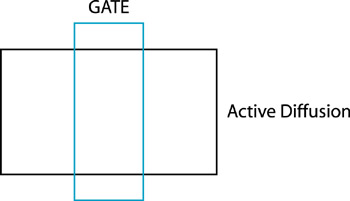
The oxide layer is often referred to as the active diffusion, or the active. The active is where atoms will be implanted to create a transistor. The overlap of the Gate and Active layers determine the size of the device. Any surplus Gate material or active that lies outside the area of the other has no effect.
The question is, "How do we know how big to make our devices to achieve the circuit performance we require? How much overlap do...