RF System Design of Transceivers for Wireless Communications

Addressing specifications that are critical for the design process, this book develops systematic methods for RF systems design, complete with a comprehensive set of design formulas.
For an ADC operating in BB oversampling at a rate f s the output noise is dominated by its quantization noise. As discussed in Chapter 2, the quantization noise is represented by
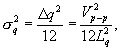
where ?q is quantization step or quantile interval (see Section 2.4.2), V p-p is the peak-to-peak voltage swing in volt, L q is the number of quantization levels defined in (2.4.24). Assuming that the quantization noise uniformly distributes over frequency 0 to f s /2, the quantization noise density P Nq is
| (3D.1) |  |
However, in the case of band-pass sampling a signal with the highest frequency of interest f H, the resultant quantization noise density increases approximately (2 f H / f s) times due to aliasing , and it turns into
| (3D.2) | 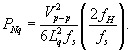 |
When the sampling frequency is in hundreds MS/s, the noise resulted from the sampling clock jitter has significant contribution to the overall ADC output noise. The jitter noise density P Nj can be expressed as
| (3D.3) | |
In this equation, P S is the sampled signal power, and it is equal to A 2 /2 for a sinusoidal signal with an amplitude A volts across an unit resistor, ![]() is the variance of angular aperture error, and the sinusoidal signal with a frequency f c has a form
is the variance of angular aperture error, and the sinusoidal signal with a frequency f c has a form
| (3D.4) | |
where ? j is the standard deviation of the sampling clock time...