Linear Circuit Design Handbook

Section 6-1: DAC Architectures

Section 6-1: DAC Architectures

DACs or D/As Introduction

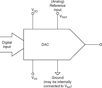
What we commonly refer to as a DAC today is typically quite a bit more. The DAC will typically have the converter itself and a collection of support circuitry built into the chip (Figure 6-1).


Figure 6-1: The basic DAC

The first DACs were board level designs, built from discrete components, including vacuum tubes as the switching elements. Monolithic DACs began to appear in the early 1970s. These early examples were actually sub-blocks of the DAC. An example of this would be the AD550, which was a 4 bit binarily weighted current source. This current source block would be mated to a separate part, such as the AD850, which contained a resistor array and complementary-MOS (CMOS) switches. Together these would form the basic DAC. As we moved on in time these functions were integrated on the same die, additional digital circuitry, specifically latches to store the digital input, were added. Then a second rank of latches were often added. The purpose of the second rank was to allow the microprocessor or microcontroller to write many DACs in a system and update them all at the same time. The input rank of latches could also be a shift register, which would allow a serial interface.

On the back end, since the output of the DAC is often a current, an op amp is often added to perform the current-to-voltage (I/V) conversion. On the front end a voltage reference is often added.

Process limitations...

UNLIMITED FREE
ACCESS
TO THE WORLD'S BEST IDEAS

SUBMIT
Already a GlobalSpec user? Log in.

This is embarrasing...

An error occurred while processing the form. Please try again in a few minutes.

Customize Your GlobalSpec Experience

Category: Digital-to-Analog Converter (DAC) Chips
Finish!
Privacy Policy

This is embarrasing...

An error occurred while processing the form. Please try again in a few minutes.