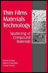
Thin Film Materials Technology: Sputtering of Compound Materials
Many of the technological advances in LSI (large-scale integration) through ULSI (ultra large-scale integration) integrated circuits can be traced to advances in thin-film processing techniques. These advances have allowed the development of many kinds of thin-film electronic devices including thin-film transistors, surface acoustic devices, high-precision resistors, solar cells, magnetic and/or optical memory, LCD (liquid crystal display) and plasma displays, and a variety of sensors and actuators.
Most of these thin films are widely used not only for information devices but also for energy and environmental systems like ecological buildings. Table 5.1 shows typical thin-film materials used for these applications. Compound thin films are also important for these practical applications, as seen in the table.
| Application | Materials | |
|---|---|---|
| Electronics | electrodes, interconnections | Au, Al, Cu, Cr, Ti, Pt, Mo, W, Al/Si, Pt/Si, Mo/Si. |
| resistors | Cr, Ta, Re, TaN, TiN, NiCr, SiCr, TiCr, SnO 2, In 2O 3. | |
| dielectrics | AIN, BN, Si 3N 4, Al 2O 3, BeO, SiO, SiO 2, TiO 2, Ta 2O 5, HfO 2, PbO, MgO, Nb 2O 5, Y 2O 3, ZrO 2, BaTiO 3, LiNbO 3, PbTiO 3, PLZT, ZnS. | |
| insulators | Si 3N 4, Al 2O 3, SiO, SiO 2, TiO 2, Ta 2O 5. | |
| magnetics | Fe, Co, Ni, Ni ?Fe, Te ?Fe, GdCo. | |
| superconductors | Nb, NbN, Nb 3Sn,... |