 | This text/reference provides students and practicing engineers with an introduction to the classical methods of designing electrical circuits, but incorporates modern logic design techniques used in the latest microprocessors, microcontrollers, microcomputers, and various LSI components. The book provides a review of the classical methods e.g., the basic concepts of Boolean algebra, combinational logic and sequential logic procedures, before engaging in the practical design approach and the use of computer-aided tools. The book is enriched with numerous examples (and their solutions), over 500 illustrations, and includes a CD-ROM with simulations, additional figures, and third party software to illustrate the concepts discussed in the book. |
Digital Principles & Logic Design
Chapter 11 - Logic Family
Logic gates and memory devices are fabricated as integrated circuits (ICs) because the components used, such as resistors, diodes, bipolar junction transistors, and the insulated gate or metal-oxide semiconductor field-effect transistors are the integral parts of the chip. The various components are interconnected within the chip to form an electronic circuit during assembly. The chip is mounted on a metal or plastic package, and connections are welded to the external pins to form an IC. The ICs result in an increase in reliability and reduction in weight and size.
Small-scale integration (SSI) refers to ICs housing fewer than 10 gates in a single chip. Medium-scale integration (MSI) includes 11 to 100 gates, whereas large-scale integration (LSI) refers to more than 100 to 5000 gates in a single chip. Very large-scale integration (VLSI) devices contain several thousands of gates per chip.
Integrated circuits are classified into two general categories - (a) linear and (b) digital. Linear integrated circuits are operated with continuous signals and are used to construct electronic circuits such as amplifiers, voltage comparators, voltage regulators, etc. Digital circuits are operated with binary signals and are invariably constructed with integrated circuits. This chapter describes the basic internal structure of different types of logic families and analysis of their operation.
The various logic families can be broadly classified into categories according to the IC fabrication process - (a) bipolar and (b) metal oxide semiconductor (MOS). Integrated circuits are available in various types of packages as mentioned below.
- (i) Dual-in-Line Package or DIP
- (ii) Leadless Chip Carrier or LCC
- (iii) Plastic Leaded Chip carrier or PLCC
- (iv) Plastic QUAD Flat Package or PQFP
- (v) Pin Grid Array or PGA
According to the internal construction and fabrication process involved in the integrated circuits, they are placed in different logic families as follows.
| RTL | Resistor-transistor logic |
| DTL | Diode-transistor logic |
| TTL | Transistor-transistor logic |
| ECL | Emitter-coupled logic |
| I2L | Integrated-injection logic |
| MOS | Metal oxide semiconductor |
| CMOS | Complementary metal oxide semiconductor |
The first two, RTL and DTL logic families have only historical significance, since they are seldom used in new designs. RTL was the first commercially available family to have been used extensively. It is included here because it represents a useful starting point to understand the basic operation of digital gates. A TTL circuit is the modification of a DTL and hence, DTL circuits have been gradually replaced by TTL. The operation of TTL will be easier to understand after DTL gates are discussed. These families have a large number of SSI circuits as well as MSI and LSI circuits. I2L and MOS are mostly used for the construction of LSI functions.
The basic circuit in each digital IC logic family is either a NAND or a NOR gate. Combinational logic functions and more complex functions are generated using this basic circuit, which may be referred to as the primary building block. As an example, an RS latch is constructed from two NAND gates or two NOR gates connected back to back. A master-slave flip-flop is obtained from the interconnection of about ten logic gates. Each of the logic families provides numerous types of ICs that perform different types of logic functions. The differences in the logic functions available from different logic families are not so much in the function that they achieve, but they are different in specific characteristics of the basic building blocks from which the functions are constructed.
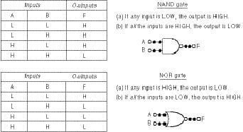
Figure 11.1
NAND and NOR gates are usually defined by the Boolean functions in terms of binary variables. While analyzing them as electronic circuits, it is more convenient to investigate their input-output relationship in terms of two voltage levels-high level (H) and low level (L) (refer to section 3.11). Binary variables use the logic values of 1 and 0. When positive
logic is adopted, the high-voltage level is assigned the binary value of logic 1 and the low-voltage level is a binary 0. From the truth table of a positive logic NAND gate, we deduce its behavior in terms of high and low levels as indicated in Figure 11.1. The corresponding behavior of the NOR gate is also stated in the same figure. These statements must be remembered because they will be used during the analysis of all gates in this chapter.
© 2006-2024 Infinity Science Press. All rights reserved.