 | This text/reference provides students and practicing engineers with an introduction to the classical methods of designing electrical circuits, but incorporates modern logic design techniques used in the latest microprocessors, microcontrollers, microcomputers, and various LSI components. The book provides a review of the classical methods e.g., the basic concepts of Boolean algebra, combinational logic and sequential logic procedures, before engaging in the practical design approach and the use of computer-aided tools. The book is enriched with numerous examples (and their solutions), over 500 illustrations, and includes a CD-ROM with simulations, additional figures, and third party software to illustrate the concepts discussed in the book. |
Digital Principles & Logic Design
Section 6.4.1 - Design Procedure with PLA
In the case of ROM-based design, we have seen that, since all the minterms are generated in a ROM, the realization of a set of Boolean functions is based on minterms canonical expressions. It is never necessary to minimize the expressions prior to obtaining the realization with a ROM. On the other hand, in the case of PLA, the product terms generated are not necessarily the minterms, as these product terms depend upon how the fuses are programmed. As a consequence, the realization using PLA is based on the sum of the products expressions. Also, it is significant that the number of product terms is limited for a PLA and the logic designer must utilize them most intelligently. This implies that it is necessary to obtain a set of expressions in such a way that the number of product terms does not exceed the number of AND gates in the PLA. Therefore, some degree of simplification of Boolean functions is needed. Several techniques of minimization of Boolean expressions have already been discussed in earlier chapters.
Example 6.4. To demonstrate the use of PLA to implement combinational logic circuits, consider the following expression
F1 ( A, B, C) = (0, 1, 3, 4) and
F2 ( A, B, C) = (1, 2, 3, 4, 5).

Figure 6.16(a) Map for function F1. - Figure 6.16(b) Map for function F2.
Assume that a 3 × 4 × 2 PLA is available for the realization of the above functions. It should be noted that according to the number of inputs and output, the specified PLA is sufficient to realize the functions. However, total distinct minterms in the functions are six, whereas available product terms or the number of AND gates in the specified PLA is four. So some simplification or minimization is required for the functions. Karnaugh maps are drawn in Figures 6.16(a) and 6.16(b) for this purpose.
The simplified Boolean expressions for the functions are
F1 = B'C' + A'C and
F2 = A'B + A'C + AB'.
In these expressions, there are four distinct product terms-B'C', A'C, A'B, and AB'. So these function can be realized by the specified 3 × 4 × 2 PLA. The internal connection diagram for the functions using PLA after fuse-links programming is demonstrated in Figure 6.17.
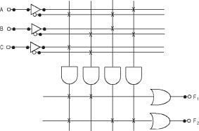
Figure 6.17
Programming the PLA means to specify the paths in its AND-OR-INVERT pattern. A PLA program table is a useful tool to specify the input-output relationship indicating the number of product terms and their expressions. It also specifies whether the output is complemented or not. The program table for the above example is shown in Figure 6.18.
|
Product Terms | Inputs | Outputs | |||||
| A | B | C | F1 | F2 | |||
| A'B | 1 | 0 | 1 | - | - | 1 | |
| A'C | 2 | 0 | - | 1 | 1 | 1 | |
| AB' | 3 | 1 | 0 | - | - | 1 | |
| B'C' | 4 | - | 0 | 0 | 1 | - | |
| T | T | T/C | |||||
Figure 6.18
The first column lists the product terms numerically. The second column specifies the required paths between inputs and AND gates. The third column indicates the paths between the AND gates and OR gates. Under each output variable, T is written if output INVERTER is bypassed i.e., the output at true form, and C is written if output is complemented with INVERTER. The Boolean terms listed at the leftmost are for reference only, they are not part of the table.
For each product term, the inputs are marked with 1, 0, or - (dash). If the input variable is present in the product term at its uncomplemented form, the corresponding input variable is marked with a 1. If the input variable appears in the product term at its complemented form, it is marked with a 0. If the variable does not at all appear in the product term, it is marked with a - (dash). Thus the paths between the inputs and the AND gates are specified under the column heading inputs and accordingly the links at the inputs of AND gates are to be retained or blown off. The AND gates produce the required product term. The open terminals of AND gates behave like logic 1.
The paths between the AND gates and OR gates are specified under the column heading outputs. Similar to the above, the output variables are also marked with 1, 0, or - (dash) depending upon the presence of product terms in the output expressions. Finally, a T (true) output dictates that links across the INVERTER are retained and for C (complemented) at output indicates that the link across the INVERTER is to be broken. The open terminals of OR gates are assumed to be logic 0.
While designing a digital system with PLA, there is no need to show the internal connections of the unit. The PLA program table is sufficient to specify the appropriate paths. For a custom made PLA chip this program table is needed to provide to the manufacturer.
Since for a given PLA, the number of AND gates is limited, careful investigation must be carried out, while implementing a combinational circuit with PLA, in order to reduce the total number of distinct product terms. This can be done by simplifying each function to a minimum number of terms. Note that the number of literals in a term is not important as all the inputs are available. It is required to obtain the simplified expressions both of true form and its complement form for each of the functions to observe which one can be expressed with fewer product terms and which one provides product terms that are common to other functions. The following example will clarify this.
Example 6.5. Implement the following Boolean functions using a 3 × 4 × 2 PLA.
F1 ( A, B, C) = (3, 5, 6, 7) and
F2 ( A, B, C) = (0, 2, 4, 7).
Solution. A total of seven minterms are present in the two functions above, whereas the number of AND gates is four in the specified PLA. So simplification of the above functions is necessary. Simplification is carried out for both the true form as well as the complement form for each of the functions. Karnaugh maps are drawn in Figure 6.19(a)-(d).

Figure 6.19(a) Map for function F1. - Figure 6.19(b) Map for function F2.

Figure 6.19(c) Map for function F1'. - Figure 6.19(d) Map for function F2'.
The Boolean expressions are
F1 = AC + AB + BC and F2 = B'C' + A'C' + ABC
F1' = B'C' + A'B' + A'C' and F2' = A'C + B'C + ABC'.
From the Boolean expressions it can be observed that if both the true forms of F1 and F2 are selected for implementation, the total number of distinct product terms needed to be realized is six, which is not possible by the specified 3 × 4 × 2 PLA. However, if F1' and F2 are selected, then the total number of distinct product terms reduces to four, which is now possible to be implemented by the specified PLA. F1 can be complemented by the output INVERTER to obtain its true form of F1. The PLA program table for these expressions is prepared in Figure 6.20. Note that the C (complement) is marked under the output F1 indicating that output INVERTER exists at the output path of F1. The logic diagram for the above combinational circuit is shown in Figure 6.21.
| Product Terms | Inputs | Outputs | |||||
| A | B | C | F1 | F2 | |||
| B'C' | 1 | - | 0 | 0 | 1 | 1 | |
| A'B' | 2 | 0 | 0 | - | 1 | - | |
| A'C' | 3 | 0 | - | 0 | 1 | 1 | |
| ABC | 4 | 1 | 1 | 1 | - | 1 | |
| C | T | T/C | |||||
Figure 6.20
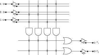
Figure 6.21
It should be noted that the combinational circuits for the examples presented here are too small and simple for practical implementation with PLA. But they do serve the purpose of demonstration and show the concept of PLA combinational logic design. A typical commercial PLA would have over 10 inputs and about 50 product terms. The simplification of so many variables are carried out by means of tabular method or other computer-based simplification methods. Thus, the computer program assists in designing the complex digital systems. The computer program simplifies each of the functions of the combinational circuit and its complements to a minimum number of terms. Then it optimizes and selects a minimum number of distinct product terms that cover all the functions in their true form or complement form.
© 2006-2026 Infinity Science Press. All rights reserved.