 | This text/reference provides students and practicing engineers with an introduction to the classical methods of designing electrical circuits, but incorporates modern logic design techniques used in the latest microprocessors, microcontrollers, microcomputers, and various LSI components. The book provides a review of the classical methods e.g., the basic concepts of Boolean algebra, combinational logic and sequential logic procedures, before engaging in the practical design approach and the use of computer-aided tools. The book is enriched with numerous examples (and their solutions), over 500 illustrations, and includes a CD-ROM with simulations, additional figures, and third party software to illustrate the concepts discussed in the book. |
Digital Principles & Logic Design
Section 6.3.1 - Implementation of Combinational Logic Circuits
The implementation of Boolean functions using decoders was already discussed in Chapter 5. The same approach is applicable in using ROM, since ROM is the device that includes both a decoder and OR gates within the same chip. Given a set of Boolean expressions in minterms canonical form or a set of expressions in truth table form, first it is only necessary to select a ROM according to the input variables and number of output lines, and then to identify which links of the ROM are to be retained and which are to be blown. The blowing off of appropriate fuses or opening the links is referred to as programming. The designer needs only to specify a ROM program table that provides information for the required paths in the ROM. Some examples of ROM-based design are demonstrated here.
Example 6.1. Consider that the following Boolean functions are to be developed using ROM.
F1 (A, B, C) = ( 0,1,2,5,7) and
F2 (A, B, C) = (1,4,6).
When a combinational circuit is developed by means of a ROM, the functions must be expressed in the sum of minterms or by a truth table. The truth table of the above functions is shown in Figure 6.6. Since there are three input variables, a ROM containing a 3-to-8 line decoder is needed. In addition, since there are two output functions, the OR array must contain at least two OR gates. That means, a 23 × 2 ROM or 8 × 2 ROM is to be employed to realize the above functions. The logic diagram of the ROM after blowing off the appropriate fuses is illustrated in Figure 6.7. Obviously, this is too simple a combinational circuit to be implemented with a ROM. This example is merely for illustration purpose only. From the practical point of view, the real advantage of a ROM is in implementation of complex combinational networks having a large number of inputs and outputs.
Some ROM units are available with INVERTERs after each of the OR gates and they are specified as having initially all 0s at their outputs. The programming procedure in such ROMs require to blow off the link paths of the minterms (or addresses) that specify an output of 1 in the truth table. The outputs of the OR gates will then generate the complements of the functions, but the INVERTERs placed after OR gates complement the functions once more to provide the desired outputs. This is shown in Figure 6.8 for implementation of the logic functions as described in the previous example.
Decimal Equivalent | Input Variables | Outputs | |||
| A | B | C | F1 | F2 | |
| 0 | 0 | 0 | 0 | 1 | 0 |
| 1 | 0 | 0 | 1 | 1 | 1 |
| 2 | 0 | 1 | 0 | 1 | 0 |
| 3 | 0 | 1 | 1 | 0 | 0 |
| 4 | 1 | 0 | 0 | 0 | 1 |
| 5 | 1 | 0 | 1 | 1 | 0 |
| 6 | 1 | 1 | 0 | 0 | 1 |
| 7 | 1 | 1 | 1 | 1 | 0 |
Figure 6.6
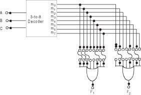
Figure 6.7
The previous example demonstrates the general procedure for implementing any combinational circuit with a ROM. From the number of inputs and outputs, the size of the ROM is determined first and then the programming for blowing off the appropriate fuse links is required with the help of the truth table or minterms. No further manipulation or simplification of Boolean functions is required. In practice, while designing with ROM, it is not essential to show the internal gate connections of links inside the unit. The designer simply has to specify the particular ROM and provide the ROM truth table as in Figure 6.6. The truth table provides all the information for programming of ROM. No internal logic diagram is necessary to accompany the truth table.

Figure 6.8
Example 6.2.Find the squares of 3-bit numbers.
Solution. This example has already been discussed and implemented with the classical method in Chapter 5. There are three input variables and six output functions. To implement with ROM, a 23 × 6 ROM or 8 × 6 ROM is required. The truth table is again shown in Figure 6.9 for convenience. Figure 6.10 shows the inputs and outputs with ROM and the internal fusible junctions are shown in Figure 6.11 after programming.
Input variables | Output variables | |||||||||
| Decimal | X | Y | Z | Decimal | A | B | C | D | E | F |
| 0 | 0 | 0 | 0 | 0 | 0 | 0 | 0 | 0 | 0 | 0 |
| 1 | 0 | 0 | 1 | 1 | 0 | 0 | 0 | 0 | 0 | 1 |
| 2 | 0 | 1 | 0 | 4 | 0 | 0 | 0 | 1 | 0 | 0 |
| 3 | 0 | 1 | 1 | 9 | 0 | 0 | 1 | 0 | 0 | 1 |
| 4 | 1 | 0 | 0 | 16 | 0 | 1 | 0 | 0 | 0 | 0 |
| 5 | 1 | 0 | 1 | 25 | 0 | 1 | 1 | 0 | 0 | 1 |
| 6 | 1 | 1 | 0 | 36 | 1 | 0 | 0 | 1 | 0 | 0 |
| 7 | 1 | 1 | 1 | 49 | 1 | 1 | 0 | 0 | 0 | 1 |
Figure 6.9M

Figure 6.10

Figure 6.11
Example 6.3.Design a code converter circuit for BCD-to-Excess-3 as well as BCD-to-2421 code using ROM.
Solution.
| Decimal | BCD code | Excess-3 code | 2421 code | |||||||||
| Equivalent | A | B | C | D | W | X | Y | Z | P | Q | R | S |
| 0 | 0 | 0 | 0 | 0 | 0 | 0 | 1 | 1 | 0 | 0 | 0 | 0 |
| 1 | 0 | 0 | 0 | 1 | 0 | 1 | 0 | 0 | 0 | 0 | 0 | 1 |
| 2 | 0 | 0 | 1 | 0 | 0 | 1 | 0 | 1 | 0 | 0 | 1 | 0 |
| 3 | 0 | 0 | 1 | 1 | 0 | 1 | 1 | 0 | 0 | 0 | 1 | 1 |
| 4 | 0 | 1 | 0 | 0 | 0 | 1 | 1 | 1 | 0 | 1 | 0 | 0 |
| 5 | 0 | 1 | 0 | 1 | 1 | 0 | 0 | 0 | 1 | 0 | 1 | 1 |
| 6 | 0 | 1 | 1 | 0 | 1 | 0 | 0 | 1 | 1 | 1 | 0 | 0 |
| 7 | 0 | 1 | 1 | 1 | 1 | 0 | 1 | 0 | 1 | 1 | 0 | 1 |
| 8 | 1 | 0 | 0 | 0 | 1 | 0 | 1 | 1 | 1 | 1 | 1 | 0 |
| 9 | 1 | 0 | 0 | 1 | 1 | 1 | 0 | 0 | 1 | 1 | 1 | 1 |
Figure 6.12
Here, two code converter circuits are housed in one single device. There are four input variables and eight output lines (four outputs for Excess-3 and four outputs for 2421). Therefore, the ROM size required is 24 × 8 or 16 × 8. The combined truth table is presented in
Figure 6.12. A logic diagram with PLD notation using ROM is given in Figure 6.13.
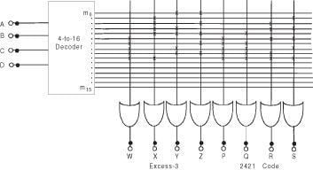
Figure 6.13
© 2006-2026 Infinity Science Press. All rights reserved.