 | This text/reference provides students and practicing engineers with an introduction to the classical methods of designing electrical circuits, but incorporates modern logic design techniques used in the latest microprocessors, microcontrollers, microcomputers, and various LSI components. The book provides a review of the classical methods e.g., the basic concepts of Boolean algebra, combinational logic and sequential logic procedures, before engaging in the practical design approach and the use of computer-aided tools. The book is enriched with numerous examples (and their solutions), over 500 illustrations, and includes a CD-ROM with simulations, additional figures, and third party software to illustrate the concepts discussed in the book. |
Digital Principles & Logic Design
Section 6.4 - Programmable Logic Array (PLA)
A combinational network may occasionally contain don't-care conditions. During the ROM implementation of this combinational circuit, this don't-care condition also forms an address input that will never occur. The words at the don't-care addresses need not be programmed and may be left in their original state of all 0s or all 1s. Since some of the bit patterns are not at all used, the address locations corresponding to don't-care conditions are considered a waste of memory.
Consider the simple case for Example 6.3, where code conversation from BCD to
Excess-3 as well as 2421 code is demonstrated. It may be noted that for four input lines and eight output lines a 16 × 8 ROM has been used. This device has 16 addresses, though only 10 addresses are used because six addresses are attributed to don't-care conditions. That means, six words or 6 × 8 bit locations are wasted.
For the cases where don't-care conditions are excessive, it is more economical to use a second type of LSI device called a Programmable Logic Array or PLA. A PLA is similar to a ROM in concept. However, a PLA does not contain all AND gates to form the decoder or does not generate all the minterms like ROM. In the PLA, the decoder is replaced by a group of AND gates with buffers/inverters, each of which can be programmed to generate some product terms of input variable combinations that are essential to realize the output functions. The AND and OR gates inside the PLA are initially fabricated with the fusible links among them. The required Boolean functions are implemented in sum of the products form by opening the appropriate links and retaining the desired connections.
A block diagram of the PLA is shown in Figure 6.14. It consists of n inputs, m outputs, p product terms, and m sum terms. The product terms are obtained from an AND array containing p number of AND gates and the sum terms are developed by an OR array consisting of m number of OR gates. Fusible links are provided to each of the inputs of each of the AND gates as well as the OR gates. Additionally, outputs are provided with an INVERTER array with fusible links, so that the outputs are available at uncomplemented form as well as at complemented form. Therefore, the function is implemented in either AND-OR form when the output link across INVERTER is in place, or in AND-OR-INVERT form when the link is blown off. The general structure of a PLA with internal connections is shown Figure 6.15.
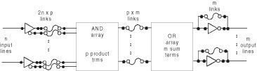
Figure 6.14

Figure 6.15
The size of a PLA is specified by the number of inputs, the number of product terms, and the number of outputs. The number of sum terms is equal to the number of outputs. The PLA described in Figure 6.14 or Figure 6.15 is specified as n × p × m PLA. The number of programmable links is 2n × p + p × m + m, whereas that of ROM is 2n × m. A typical PLA of 16 × 48 × 8 has 16 input variables, 48 product terms, and 8 output lines.
A comparison between ROM and PLA can be made to show how reduction in the number of gates is possible in PLA. Consider a typical example of implementation of a combinational circuit of 16 inputs, 8 outputs, and no more than 48 product terms. A 16 × 48 × 8 PLA can serve the purpose, which consists of 48 product terms. To implement the same combinational circuit, a 216 × 8 ROM is needed, which consists of 216 = 65536 minterms or product terms. So there is a drastic reduction in number of AND gates within the chip, thus reducing the fabrication time and cost. It should be noted that both complemented and uncomplemented inputs, i.e., 2n number of inputs appear at each AND gate providing maximum flexibility in product term generation.
Like a ROM, the PLA may also be mask-programmable or field programmable. For a mask-programmable PLA, the user must submit a PLA program table to the manufacturer to produce a custom made PLA that has the required internal paths between inputs and outputs. The second type of PLA available is called a field programmable logic array or FPLA. The FPLA can be programmed by the users by means of certain recommended procedures. Programmer equipment is available commercially for use in conjunction with certain FPLAs.
© 2006-2026 Infinity Science Press. All rights reserved.