Oscillator Design and Computer Simulation, Second Edition
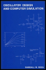
Chapter 5: Biasing

A complete and rigorous description of biasing techniques, including all temperature and leakage effects, for bipolar, JFET, dual-gate FET, and hybrid devices, is beyond the scope of this chapter. Except in rare applications, such as calibrated output-level oscillators, the bias schemes given here provide a more than adequate degree of bias point definition and stability. An active bipolar bias network is given as the final bias example. Resorting to even this modest level of bias network complexity is seldom required.

5.1 Bipolar Transistor Biasing

The bipolar junction transistor is biased in the active region with the base-emitter junction forward biased and the base-collector junction reverse biased. The base-emitter voltage is approximately 0.6 volt but increases with a decrease in temperature and with increasing current.

The required base current is the collector current divided by ?. ? increases with an increase in temperature. ? is typically 30 to 80 for RF and microwave transistors at room temperature. Greater variation in ?, even for devices of the same type, is frequently encountered. ? is also a function of collector current. It has a broad maximum at a current that is optimum for highest gain. ? drops off at lower current. Operation at currents less than the maximum gain current is often used to reduce transistor noise. ? drops off more quickly above the maximum gain current. Device data sheets normally specify expected ? for various operating conditions.

Saturation occurs when the base drive exceeds...

UNLIMITED FREE
ACCESS
TO THE WORLD'S BEST IDEAS

SUBMIT
Already a GlobalSpec user? Log in.

This is embarrasing...

An error occurred while processing the form. Please try again in a few minutes.

Customize Your GlobalSpec Experience

Category: Bipolar RF Transistors
Finish!
Privacy Policy

This is embarrasing...

An error occurred while processing the form. Please try again in a few minutes.