Oscillator Design and Computer Simulation, Second Edition
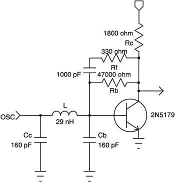
Figure 2-3 shows the schematic of the cascade used to compute the open-loop response given in Figure 2-2. A pi-network resonator is cascaded with a common-emitter 2N5179 bipolar NPN transistor amplifier. R c is the collector DC load resistance and R b provides base bias. R f is an RF feedback resistor which is decoupled for biasing through a 1000 pF capacitor. The output 1000 pF capacitor is used for DC decoupling of the collector and base when the oscillator is finally formed by connecting the output to the input.
A characteristic of well-designed oscillators is a gain peak near the phase zero crossing frequency. A second desirable characteristic is a phase-zero-crossing near the maximum phase slope. These criteria are approximately satisfied in this example with the gain peak and maximum phase slope occurring near 102 MHz. The gain margin is large for this example, ensuring that variations in production transistor parameters, passive component tolerances, and temperature effects are unlikely to prevent oscillation.