
Products & Services
See also: Categories | Featured Products | Technical Articles | More Information-
Supplier: SemiProbe
Description: SemiProbe IRIS inspection systems inspect, locate and identify defects created during wafer manufacturing, probing, bumping, dicing or general handling, providing microelectronic device manufacturers with accurate, timely quality assurance and process information. The IRIS
- Measurements: Area Mapping, Defects / ADC, Electrical Test - Parametric / In-line, Particle Contamination
- Mounting / Loading: Manual Loading
- Technology: Optical / Imaging System
- Applications: Semiconductor Wafers
-
Supplier: Nanotronics Imaging
Description: The Nanotronics Imaging nSpec® is an inspection device designed for high resolution microscopy and detection of wafer defects. With particular application in silicon carbide and Galium Nitride epi wafers, the nSpec® offers fast quantification and qualification of defects with
- Measurements: Defects / ADC
- Mounting / Loading: Manual Loading
- Technology: Optical / Imaging System
- Applications: Semiconductor Wafers
-
Supplier: Accuris
Description: Semiconductor devices - Non-destructive recognition criteria of defects in silicon carbide homoepitaxial wafer for power devices - Part 2: Test method for defects using optical inspection
-
-
Supplier: Accuris
Description: Semiconductor devices \x96 Non-destructive recognition criteria of defects in silicon carbide homoepitaxial wafer for power devices Part 2: Test method for defects using optical inspection
-
Description: IEC 63068-2:2019(E) provides definitions and guidance in use of optical inspection for detecting as-grown defects in commercially available 4H-SiC (Silicon Carbide) epitaxial wafers. Additionally, this document exemplifies optical images to enable the detection and
-
Supplier: Daitron Co., Ltd.
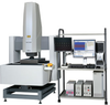
Description: The inspection and evaluation are automatically performed by placing devices on the stage and making the initial setting. The visual inspection machine is for the inspection of the top surface only, but we also offer the models for automatic inspection up to six sides.
- Mounting / Loading: Floor Mounted / Stand-alone
- Form Factor: Monitor / Instrument
- Technology: Optical / Imaging System
- Applications: Semiconductor Wafers
-
Supplier: Nikon Metrology
Description: The NWL200 series is the first lineup of wafer loaders for inspection microscopes capable of loading 100 micron thin wafers. Thanks to a new chuck system, the NWL200 series achieves highly reliable loading suitable for inspection of next-generation semiconductors.
- Maximum Wafer / Part Size: 200 mm
- Measurements: Defects / ADC
- Mounting / Loading: Floor Mounted / Stand-alone
- Features: Non-contact, Non-destructive, Other
-
Supplier: ASTM International
Description: 1.1 This practice covers an inspection procedure for determining the surface quality of silicon wafers that have been polished on one side. 1.2 This practice is intended as a large-volume acceptance method and as such does not require use of a microscope or other optical
-
Supplier: ASTM International
Description: This standard was transferred to SEMI (www.semi.org) May 2003 1.1 This practice covers an inspection procedure for determining the surface quality of silicon wafers that have been polished on one side. 1.2 This practice is intended as a large-volume acceptance method and does not
-
Supplier: Evident Scientific
Description: The Olympus MX51 industrial inspection microscope is cost-effective and optimized for the inspection requirements of a variety of electronic components, wafers and large samples.
- Total Magnification: 1.25 to 150 X
- Resolution: 100,000 nm
- Grade: Benchtop
- Eyepiece Style: Binocular
-
Supplier: Nikon Metrology
Description: series performs exceptionally precise optical inspection of wafers, photo masks, reticles and other substrates. 3 Models to Choose From L200: Offers 200mm wafer and mask inspection capabilities for reflected light illumination defect identification with various
- Total Magnification: 1 to 150 X
- Grade: Benchtop
- Remote Interface: Computer Interface, Image Analysis Processing Software
- Features: Digital Display, Fine Focus, Mechanical Stage
-
Supplier: Nikon Metrology
Description: Nikon Eclipse L300N/L300ND FPD / Wafer Inspection microscopes incorporate Nikon’s renowned CFI60 infinity optics, offering the world’s highest level of optical performance. The enhanced epi-fluorescence function, which enables 365nm UV excitation, is optimal for the
- Total Magnification: 1 to 150 X
- Grade: Benchtop
- Remote Interface: Computer Interface, Image Analysis Processing Software
- Features: Digital Display, Fine Focus, Mechanical Stage
-
Supplier: Prior Scientific, Inc.
Description: automatically moves to the correct load position and activates the loader switch, notifying the loader that the shuttle's wafer chuck is in position to receive the wafer. After the wafer is transferred to the shuttle, the system senses the vacuum change and retracts the shuttle,
- Maximum X-Distance: 154 to 256 mm
- Maximum Y-Distance: 154 to 215 mm
- Minimum Step Size (Resolution): 0.04 µm
- Stage Type: Motorized Stage
-
Supplier: Avantier Inc.
Description: Avantier Inc. offers a wide range of materials, cutting edge equipment, and optic and component capabilities for custom or OEM optics and components. We have over 50 years of expertise in custom optics and custom optical component manufacturing of lenses, prisms, windows, wafers, and
- Features: Canada Only, East Asia / Pacific Only, North America, Northeast US Only, Oceania Only, United States Only
- Design Services: Optical Component Design
- Additional Services: Prototyping
-
Supplier: 3X Ceramic Parts Company Limited
Description: Ceramic Fork Aluminum Nitride Vacuum Plate for LED wafer Aluminum nitride ceramic fork have excellent physical properties such as high thermal conductivity, low dielectric constant, reliable electrical insulation, thermal expansion coefficient matched with silicon, insulation and non
- Density: 3.359997879413084 g/cc
- Thermal Conductivity: 170 W/m-K
- MOR / Flexural Strength: 58,014.7357428788 psi
- Specialty Ceramic Type: Aluminum Nitride
-
Description: IEC 63068-4:2022(E) provides a procedure for identifying and evaluating defects in as-grown 4H-SiC (Silicon Carbide) homoepitaxial wafer by systematically combining two test methods of optical inspection and photoluminescence (PL). Additionally, this document exemplifies
-
Supplier: Accuris
Description: Semiconductor devices - Non-destructive recognition criteria of defects in silicon carbide homoepitaxial wafer for power devices Part 4: Procedure for identifying and evaluating defects using a combined method of optical inspection and photoluminescence
-
Supplier: Evident Scientific
Description: Topside and backside macro inspections are also available for all wafer sizes Thin Wafer Inspection To meet the demands of thin wafer manufacturers, the new arm design of the AL120-LMB-90 model can handle a full cassette of 90 µm wafers. Serial Interface for
- Grade: Benchtop
- Eyepiece Style: Binocular
- Microscope Type: Compound
- Features: Digital Display, Mechanical Stage
-
Supplier: WDI Wise Device Inc.
Description: The LLC6 is a precise linear lens changer with 6 lens ports providing ultra fast, automatic lens changing without the need of re-qualifying the lens. It is the ideal tool for TFT-LCD and Photomask Inspection/Repair applications or other tasks where multiple optical magnifications are
- Applications: Flat Panel Displays, Semiconductor Wafers
- Mounting / Loading: In-situ / System Mounted
- Features: Non-contact, Non-destructive, Other
-
Supplier: Teledyne DALSA
Description: 67 megapixels, Genie Nano-CXP ensures robust build quality, wide operating temperature, and an unmatched feature set—all at an incredible price. Typical Applications Semiconductor wafer inspection Surface and bump inspection Electronics manufacturing 3D solder paste
- Horizontal Resolution: 4,096 to 5,120 lines
- Maximum Frame Rate: 80 to 120 fps
- Vertical Resolution: 4,096 to 5,120 lines
- Features: Auto-Lens, CMOS, Other
-
Supplier: Nikon Metrology
Description: measurements of a variety of bump heights on advanced IC packages such as wafer-level CSP, as well as for the inspection of highly complicated structures of MEMS and probe card. Key benefits Simultaneous wide-area height measurement with Nikon proprietary confocal optics 2D measurement
- Applications: Electronics or Semiconductor Inspection, Production & Quality Control
- Image Source: Optical Microscope
- System Type: Turnkey / Complete System
-
Supplier: Hypersen Technologies Co., Ltd.
Description: measurement of both transparent and opaque materials. Such as, mobile phone’s camera module and motherboard measurement,curved glass profile measurement, chip measurement,glass thickness measurement, LCD screen inspection, wafer depth/thickness inspection, glue/film thickness
- Gage / Instrument Type: Micrometer
- Gaging Technology: Optical
- Features: Optical - LED
-
Supplier: Newport MKS
Description: very high throughput stages used in wafer positioning, inspection and electronic manufacturing applications. NewDamp elastomers can be built into equipment isolation supports and even custom machinery feet. Superior Constant Natural Frequency (CNF) Design Constant Natural Frequency
- Type: Optical Table
- Features: Vibration Isolation
-
Supplier: Newport MKS
Description: two to five times better than other commercial elastomers. The high damping factor makes them ideal for supporting and damping the high acceleration amplitudes produced by very high throughput stages used in wafer positioning, inspection and electronic manufacturing applications.
- Type: Optical Table
- Features: Vibration Isolation
-
Supplier: Newport MKS
Description: two to five times better than other commercial elastomers. The high damping factor makes them ideal for supporting and damping the high acceleration amplitudes produced by very high throughput stages used in wafer positioning, inspection and electronic manufacturing applications.
- Type: Optical Table
- Features: Vibration Isolation
-
Supplier: Newport MKS
Description: throughput stages used in wafer positioning, inspection and electronic manufacturing applications. NewDamp elastomers can be built into equipment isolation supports and even custom machinery feet. Superior Constant Natural Frequency (CNF) Design Constant Natural Frequency (CNF) is a
- Type: Optical Table
- Features: Vibration Isolation
-
Supplier: Rubicon Technology
Description: Rubicon’s sapphire epi-polished wafers are ultra-flat, super clean, stress-free large diameter substrates, offered with precision orientations and offsets and wafer-to-wafer uniformity, with one or both surfaces finished. These sapphire wafers are custom designed to meet
- Width / O.D.: 7.87402 inch
- Features: Dielectric Ceramic, Electroceramics (Electrical and Electronic Ceramics), Optics / Optical Grade
- Material Type: Sapphire
-
Supplier: Avantier Inc.
Description: Custom Optics and Custom Optical Components Avantier Inc. offers a wide range of materials, cutting edge equipment, and optic and component capabilities for custom or OEM optics and components. We have over 50 years of expertise in custom optics and custom optical component
- Materials: Germanium
-
Supplier: PI (Physik Instrumente) L.P.
Description: operation. Application fields Optical alignment, wafer inspection, wafer alignment, measuring technology, inspection systems, calibration, scanning. Thanks to the friction-free motion, no particles are formed, which makes PIglide stages ideal for cleanroom
- Load Capacity: 8.992 to 269.76 lbs
- Shape: Flat, Rectangular / Square
- Design: Metric
-
Supplier: HG Optronics, Inc.
Description: applications of lasers, including machining, material processing, spectroscopy, wafer inspection, light displays, medical diagnostics, laser printing, and data storage, etc. It has been shown that Nd:YVO4 based diode pumped solid state lasers are rapidly occupying the markets
- Damage Threshold: 750,000 W/cm²
- Surface Flatness: λ/10
- Surface Quality: 10-5 Scratch / Dig
- Features: AR-Coated, Other, Other / Specialty Material
-
Supplier: SPIE - Education
Description: The measurement of light scattered by surfaces can be used to locate and identify roughness, particulates, and defects on a wide variety of materials. Applications include the inspection of silicon wafers, optics, and storage media, characterization of thin film roughness,
- Type: Course
- Technology / Subject Expertise: Design / Engineering Methods (ESDU, DFx, etc.), Photonics / Optics
- Delivery: On-site / In Plant
-
Supplier: Prior Scientific, Inc.
Description: the user to increase labor efficiency by automatically scanning your specimens and storing points for later recollection and inspection with unmatched repeatability. The H101A is ideal for scanning or inspection of slides, microtitre trays, semiconductor wafers, or metallurgical
- Maximum X-Distance: 114 mm
- Maximum Y-Distance: 75.00000000000001 mm
- Minimum Step Size (Resolution): 0.04 µm
- Stage Type: Motorized Stage
-
Supplier: PI (Physik Instrumente) L.P.
Description: (automated optical inspection). Sensor and ultrasonic tests. Semiconductor manufacturing: Wafer processing and inspection. Laser machining: Laser welding. Highly dynamic applications in precision automation, smooth scan motion, minimum tracking errors, and short settling
- Stroke or X-Axis Travel: 0.01574804 to 0.03149608 inch
- Positioning Accuracy: 0.03 to 0.04 inch/inch
- Device Type: Ball Slide
- Bearing Type: Ball/Roller Bearing
-
Supplier: PI (Physik Instrumente) L.P.
Description: is no vibration at high velocities. Nonlinearity in control behavior is avoided and any position can be controlled easily. The drive force can be set freely. Application fields Electronics assembly: Sensor and camera assembly. Noncontact inspection, X-ray inspection, and AOI (automated
- Stroke or X-Axis Travel: 15.74804 to 31.49608 inch
- Positioning Accuracy: 0.03 to 0.04 inch/inch
- Bearing Type: Ball/Roller Bearing
- Features: Electrical
-
Supplier: Zygo Corporation
Description: thermal expansion. Machining and finishing components such as positioning stages, wafer chucks, pin chucks (with lithographic patterning), bar mirrors, and light-weighted optics require special expertise. ZYGO's proprietary machining techniques enable us to fabricate stage and optical
- Services: Design Assistance, Material Selection, Testing / Inspection
- Materials: Glass Ceramic, Sapphire, Silicate / Fused Silica
- Secondary Operations: Glazing / Coating, Lapping / Polishing
- Process: Machining











Find Suppliers by Category Top
Featured Products Top
-
 technology and linear motor technology, PI's solutions are at the forefront of supporting applications like overlay metrology, thin film metrology, edge placement error (EPE) metrology, and automated optical inspection (AOI (read more)
Browse Wafer and Thin Film Instrumentation Datasheets for PI (Physik Instrumente) L.P. -
INSACO Offers Wafer Carriers With or Without Multiple Holes INSACO, Inc has become recognized as a worldwide leader in custom machined ceramic and sapphire parts for the semiconductor industry. Through this experience (read more)
Browse Glass Fabrication Services Datasheets for Insaco, Inc. -
Watch>> - Sapphire for GaAs, Indium Phosphide, & Other Semiconductors Sapphire Wafer Carriers (read more)
Browse Wafer Cassettes Datasheets for Insaco, Inc. -
. Inspection and Packaging: Wafer probing stations, wafer inspection equipment, and wafer-level packaging (WLP) carriers (read more)
Browse Wafer Chucks Datasheets for Fountyl Technologies Pte. Ltd. -
Watch>> - Sapphire for GaAs, Indium Phosphide, & Other Semiconductors Sapphire Wafer Carriers (read more)
Browse Wafer Cassettes Datasheets for Insaco, Inc. -
in wafer dicing, grinding, thin-film deposition, and automated optical inspection (AOI (read more)
Browse Wafer Chucks Datasheets for Fountyl Technologies Pte. Ltd. -
Ideal for wafer defect inspection, thin-film measurement, and optical positioning. (read more)
Browse Wafer Chucks Datasheets for Fountyl Technologies Pte. Ltd. -
Range: 80–270 MHz Scanning Angle Range: 4.9–60.5 mrad Diffraction Efficiency: >40% to >85% Applications Laser Direct Writing Wafer Inspection Precision Circuit Board Drilling Biological (read more)
Browse Laser Optics, Heads, and Beam Delivery Components Datasheets for CASTECH, Inc. -
Product Overview Used as structural support members in precision metrology equipment, wafer inspection stages, coordinate measuring machines, and optical platforms where frame rigidity and dimensional stability directly determine measurement accuracy. Fountyl silicon (read more)
Browse Silicon Carbide and Silicon Carbide Ceramics Datasheets for Fountyl Technologies Pte. Ltd. -
Industrial Laser Systems Laser Direct Writing Wafer Inspection Precision Circuit Board Processing Fiber Laser Systems Optical Sensing Scientific Research Biological Detection Optical Tweezers Quantum Technology (read more)
Browse Laser Optics, Heads, and Beam Delivery Components Datasheets for CASTECH, Inc.
Conduct Research Top
-
EETimes.com | Electronics Industry News for EEs & Engineering Managers
SEMI names president of China office The Semiconductor Equipment and Materials International (SEMI) trade group announced the promotion of Yee-Ming Ting to the position of president of its new China office. Nano-Or rolls out tabletop unit for 3D inspection Nano-Or Technologies Ltd. here introduced
More Information Top
 Indicates content that may require registration and/or purchase.

-
Towards the optical inspection sensitivity optimization of EUV masks and EUVL-exposed wafers
Following wafer exposures, the resist patterns were transferred by etch to underlying SiN layers and inspected with 193 nm optical wafer inspection tools and reviewed with scanning electron microscopes.
-
ZCP2012ISTFA02214L
Scan chain cells and nets information are extracted from design data file and converted to inline optical wafer inspection care areas.
-
EUV mask defect analysis from mask to wafer printing
A wafer is exposed with the mask, and then a optical wafer inspection follows.
-
Characterization analysis study of &mgr;-bridge defect using simulation and wafer inspection tools
inspection, STI voids have been detected using optical wafer inspection tools.[2] However, there .
-
Submicron defect detection by SEMSpec: an e-beam wafer inspection system
This maximum image processing speed is identical to that obtained on the high- speed optical wafer inspection system by KLA-Tencor.
-
Classification and Size Estimation of Wafer Defects by Using Scattered Light Distribution
Optical wafer inspection is the most effective method for detecting and classifying defects and estimating their size in a short time.
-
ZCP2012ISTFATAD526
Scan chain cells and nets information are extracted from design data file and converted to inline optical wafer inspection care areas.
-
ZCP2012ISTFATAD
Scan chain cells and nets information are extracted from design data file and converted to inline optical wafer inspection care areas.
-
DSA hole defectivity analysis using advanced optical inspection tool
This paper discusses the defect density detection and analysis methodology using advanced optical wafer inspection capability to enable accelerated development of a DSA process/process tools and the required inspection capability to monitor such a process.
-
Investigation of the performance of state-of-the-art defect inspection tools within EUV lithography
The final result is benchmarked against state-of-the-art patterned mask inspection and blank inspection to evaluate the capabilities and limitations of the optical wafer inspection .