
Products & Services
See also: Categories | Featured Products | Technical Articles | More Information-
Supplier: CoorsTek
Description: Windows are chamber lids designed to transmit RF (radio frequency) and microwave energy into the plasma etch chamber while resisting erosion from the harsh plasma etch environment. An effective window has a low loss tangent (high transmittance) across RF and microwave frequencies.
- Features: Alumina / Aluminum Oxide, Carbide Materials, Specialty Ceramic
- Specialty Ceramic Type: Aluminum Nitride, Silicon Carbide, Yttria
- Applications: Chemical / Materials Processing
- Shape / Form: Fabricated / Custom Shape
-
Supplier: Plasma Etch, Inc.
Description: Based on our popular BT-1, it shares the same robust and reliable characteristics while providing yet another example of Plasma Etch surface modification innovation. The large all aluminum chamber accommodates a generously sized circular, rotating active processing surface has the option of
- Features: Automated Loading, Gas Control Unit, Integral Process Controller, Other
- Materials Processed: Compound Semiconductors / GaAs, Metal, Tungsten / Refractory Metal
- Type: Factory / Free Standing
- Vacuum / Pressure Range: Medium (< 1, >10-3 torr)
-
Supplier: CoorsTek
Description: CoorsTek advanced, high-purity ceramic components are built to withstand the extreme environments in plasma etch (or "dry" etch) chambers — including vapor phase chemical etchants, high voltage RF (radio frequency) and microwave plasma, volatile byproducts, and aggressive cleaning
- Features: Alumina / Aluminum Oxide, Carbide Materials, Specialty Ceramic
- Specialty Ceramic Type: Aluminum Nitride, Silicon Carbide, Yttria
- Applications: Chemical / Materials Processing
- Shape / Form: Fabricated / Custom Shape
-
-
Supplier: CoorsTek
Description: components are built to withstand the extreme environments in plasma etch (or "dry" etch) chambers — including vapor phase chemical etchants, high voltage RF (radio frequency) and microwave plasma, volatile byproducts, and aggressive cleaning cycles. EXAMPLE ETCH PROCESS MATERIALS
- Features: Alumina / Aluminum Oxide, Carbide Materials, Specialty Ceramic
- Specialty Ceramic Type: Aluminum Nitride, Silicon Carbide, Yttria
- Applications: Chemical / Materials Processing
- Shape / Form: Fabricated / Custom Shape
-
Supplier: Quorum Technologies
Description: The K1050X is a modern, solid-state RF plasma barrel reactor designed to meet the requirements of research and development and small-scale production for a wide and varied range of plasma etching, plasma ashing and plasma cleaning applications. Key Features * Drawer type
- Reactor Design: Other Reactor Design
-
Supplier: 3X Ceramic Parts Company Limited
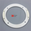
Description: Ceramic Focus Ring for Plasma Etch Equipment When aluminum alloy is selected as the chamber material of the etcher, it is easy to cause metal particle pollution. Instead, a dense anodic aluminum oxide layer is coated on the aluminum alloy to improve the corrosion resistance of the
-
Supplier: Plasma Etch, Inc.
Description: Built as an extension of our MK-II platform, it offers you the same repeatability, reliability and long life, as well as low maintenance costs. The Reactive Ion Etch (RIE) electrode offers the highest directional plasma effect. Etching with our roll to roll plasma etcher in the
- Materials Processed: Compound Semiconductors / GaAs, Metal, Tungsten / Refractory Metal
- Features: Gas Control Unit, Integral Process Controller, Other
- Vacuum / Pressure Range: Medium (< 1, >10-3 torr)
- Process: Plasma Etching / Cleaning
-
Supplier: Terra Universal, Inc.
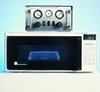
Description: First-of-its-kind design uses microwave oven to generate plasma cleaning medium Safely removes organic and many inorganic contaminants from a wide range of components and substrates Maintains low processing temperatures (25-200°C controllable) Produces higher plasma power and densities
- Temperature: 392 F
- Internal Length: 4.1 inch
- Internal Width: 4.1 inch
- Internal Depth / Height: 6 inch
-
Supplier: Hitachi High Technologies America, Inc.
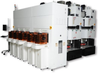
Description: support these next-generation processes. The 9000 platform incorporates HHT’s new microwave ECR(Electron Cyclotron Resonance) plasma etching chamber that is proven in high volume manufacturing usage.
- Applications: Etching - Plasma / Wet
- Mounting / Loading: Floor Mounted / Stand-alone
-
Supplier: Hitachi High Technologies America, Inc.
Description: Plasma) etch system provides superior performance in profile control as well as in higher etching rate and selectivity compared to conventional ion-milling processes. Applicable wafer diameter 150mm, 200mm
- Applications: Etching - Plasma / Wet
- Mounting / Loading: Floor Mounted / Stand-alone
-
Supplier: Hitachi High Technologies America, Inc.
Description: loss in volume production. Non-Volatile Materials Etch System E-600/8000 Series: the EMCP (Electro Magnetically Coupled Plasma) offers an outstanding solution to this problem ensuring constant high performance even for non-volatile material etch.
- Applications: Etching - Plasma / Wet
- Mounting / Loading: Floor Mounted / Stand-alone
-
Supplier: Advanced Energy Industries, Inc.
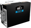
Description: Litmas is an all-in-one remote plasma source combining the power supply, LitmasMatch™ matching network, and plasma chamber into one compact chassis. Small-footprint point-of-use abatement solution Highly reliable, effective abatement with minimum utilities usage Lower cost of ownership
- Type: RF Plasma (ICP)
- Materials / Substrates: Semiconductors / Wafers
- Features: Specialty / Other
-
Supplier: Plasma Etch, Inc.
Description: Our welded aluminum vacuum chamber encloses a generous 500 square inches of active plasma processing surface. Surface modification with Plasma Etch yields increased bond strength and cleanliness of most any surface material.
- Materials Processed: Compound Semiconductors / GaAs, Metal, Tungsten / Refractory Metal
- Features: Gas Control Unit, Integral Process Controller, Other
- Type: Laboratory / Benchtop
- Vacuum / Pressure Range: Medium (< 1, >10-3 torr)
-
Supplier: Plasma Etch, Inc.
Description: As in all Plasma Etch systems a capacitive parallel plate design is used for the most effective plasma generation. Competitive units with glass/quartz barrel chambers cannot penetrate the vacuum containment vessel and therefore are restricted to inductive coupling using an RF coil
- Materials Processed: Compound Semiconductors / GaAs, Metal, Tungsten / Refractory Metal
- Features: Integral Process Controller, MEMS, Medical, Other, Photovoltaic / Solar, Research / Surface Analysis, Semiconductor Manufacturing
- Type: Laboratory / Benchtop
- Vacuum / Pressure Range: Medium (< 1, >10-3 torr)
-
Supplier: Advanced Energy Industries, Inc.
Description: Litmas is an all-in-one remote plasma source combining the power supply, LitmasMatch™ matching network, and plasma chamber into one compact chassis. Small-footprint point-of-use abatement solution Highly reliable, effective abatement with minimum utilities usage Lower cost of ownership
-
Supplier: IPS Limited
Description: Emerald green industrial plating tape for disposition, plasma, lamination, alkaline, etch, photo develop with great chemical resistance. Features/Applications: disposition plasma lamination alkeline etch photo develop
- Adhesive: Silicone
- Features: Single-Sided Adhesive
-
Supplier: Comdel, Inc.
Description: proven RF amplifier technology. Applications: The CLB series is designed to meet the performance demand in RF-driven plasma systems for semiconductor processing. Applications include etch, RIE, parallel plate, ICP, RF sputtering, CVD and PVD, as well as induction and dielectric heating
- Type: Plasma Power Supply
-
Supplier: Comdel, Inc.
Description: Proven Reliability in Plasma Vacuum Systems Worldwide Performance: The CLX series low frequency RF power supplies are available in power ranges from 600 to 10,000 Watts with fixed frequencies from 20 kHz to 2 MHz, and frequency agile capability up to 10% bandwidth. The CLX 1250 provides 1250
- AC Input Voltage: 185 to 480 volts
- Output Frequency: 2 to 30 MHz
- Number of Outputs: 1 #
- DC Output Voltage: -5 to 10 volts
-
Supplier: Comdel, Inc.
Description: Proven Reliability in Plasma Vacuum Systems Worldwide Performance: The CX series power supplies start at power ranges from 600 to 2500 Watts with fixed frequencies from 2 MHz to 30 MHz, and frequency agile capability up to 10% bandwidth. The solid-state design provides low cost of ownership
- AC Input Voltage: 115 to 480 volts
- Input Frequency: 50 to 60 Hz
- Output Frequency: 2 to 30 MHz
- Number of Outputs: 1 #
-
Supplier: Comdel, Inc.
Description: Stable, Reliable, Low Frequency Power for Industrial Heating and Plasma Processing Applications Performance: The CLF series generators provide stable process power up to 5 kW. The CLF 500 provides 500 watts of power. The half-rack supplies operate at any fixed frequency from 20 to 50 kHz. In
- AC Input Voltage: 100 to 239 volts
- Input Frequency: 50 to 60 Hz
- Output Frequency: 0.02 to 0.05 MHz
- Number of Outputs: 1 #
-
Supplier: Kayaku Advanced Materials, Inc.
Description: Thermoplastics with built-in release properties for use as etch mask for pattern transfer and the fabrication of nanopatterns Excellent properties for thermal NIL Longer life-time of anti-sticking layers on the mold High plasma etch resistance
- Applications: Electronics / Microelectronics
- Thick Film Type: Resistor
-
Supplier: MCA - Advanced Materials Division
Description: Semitron® MPR 1000 shapes possess excellent heat resistance and low rates of erosion in plasma chambers. Due to these characteristics, it is often chosen for vacuum chamber applications within etch, CVD, and ion implant sub segmentations in the semiconductor and electronics industry.
- Tensile Strength (Break): 15,000 psi
- Tensile Modulus: 1,000 ksi
- Use Temperature: 500 F
- Industry: Electronics, Semiconductors / ICs
-
Description: plasma etch equipment, primarily in the etch chamber. The rings are strategically positioned to optimize plasma distribution and maintain uniformity during the etching process. Semiconductor manufacturing processes demand operation within cleanroom environments, especially for
- Features: Alumina / Aluminum Oxide, Specialty Ceramic
-
Description: General Digital offers optical bonding and optical film laminating services to enhance the optical performance of an LCD, OLED or Plasma display. Optically bonding an LCD, OLED or Plasma display improves both optical performance and durability. Optical Bonding is the affixing of two
- Coating: Antireflection, Filter, ITO, Protective
- Materials: Glass, Polymer
- Wavelength Range: IR, Visible
- Features: North America, Northeast US Only, Other, United States Only
-
Supplier: Solid State Cooling Systems
Description: modes • Programmed for Lam Research analog and (single channel, single channel dual output or dual output Master/Slave) Applied Materials CHX plasma etcher interfaces
- Cooling Capacity: 1.2 kW
- Process Flow: 4 GPM
- Process Pressure: 33 psi
- Operating Temperature: 14 to 176 F
-
Supplier: Precision Polymer Engineering Ltd.
Description: from elastomer seals and ultra-low permeation rates. Key Material Attributes: Ultra pure with extremely low trace metal contaminants which may cause electrical yield problems. Excellent plasma resistance – ideal for most plasma chemistries except high F-radical processes. Plasma
- O-ring Size: "AS568" standard sizes (001-475), "AS568-" boss gasket sizes (901- and up), British Standard metric sizes, JIS standard sizes
- O-ring Hardness (Durometer): 65 durometer, 70 durometer, 75 durometer, 80 durometer
- Synthetic Rubbers: Fluoroelastomer (FKM), Perfluoroelastomer (FFKM, FFPM)
-
Supplier: Precision Polymer Engineering Ltd.
Description: from elastomer seals and ultra-low permeation rates. Key Material Attributes: Ultra pure with extremely low trace metal contaminants which may cause electrical yield problems. Excellent plasma resistance – ideal for most plasma chemistries except high F-radical processes. Plasma
- O-ring Size: "AS568" standard sizes (001-475), "AS568-" boss gasket sizes (901- and up), British Standard metric sizes
- O-ring Hardness (Durometer): 65 durometer, 70 durometer, 75 durometer, 80 durometer
- Synthetic Rubbers: Fluoroelastomer (FKM), Perfluoroelastomer (FFKM, FFPM)
-
Supplier: Precision Polymer Engineering Ltd.
Description: Nanofluor® Y75G is a highly fluorinated elastomer which incorporates relatively low levels of an advanced nanoparticle type filler system, producing a clean compound formulated for minimum particle generation. Nanofluor® Y75G has been tested in various plasma types and sources and benchmarked
-
Supplier: Kayaku Advanced Materials, Inc.
Description: KMPR® 1000 develops in standard aqueous TMAH developers and can be removed more easily after fabrication compared to traditional epoxy resists. Available in five viscosities, KMPR® 1000 enables single‑coat thicknesses from 4–110 μm. With excellent adhesion, as well as strong chemical and
- Applications: Electronics / Microelectronics
- Thick Film Type: Resistor
-
Supplier: Surventis Surface Treatment LLC
Description: Gardacid P 4462/1 is a liquid sulfuric acidic pickling product used to remove laser and plasma cutting scale and rust from ferrous substrates. Gardacid P 4462/1 can also be used to clean and etch aluminum substrates. A fluoride additive is sometimes used with aluminum. The carefully balanced
- Type: Etchant / Pickle, Rust / Corrosion Remover, Strong Acid / Mineral Acid Cleaner (0 to 2 pH), Surface Treatment
-
Supplier: Microchip Technology, Inc.
Description: to 2MHz High voltage pulsed DC AM transmitters Plasma deposition/etch Series Gate Resistance (Rg) <0.1 ohm Tr and Tf times of <10ns Industry's Lowest Gate Charge Fast switching, uniform signal propagation Pulse power applications Fast switching, reduced gate drive power
-
Supplier: PTB Sales, Inc.
Description: throughput pumps incorporating a hybrid pumping mechanism for higher gas flow. These are optimized for processes such as plasma etch. We also offer repair service.
-
Supplier: ASTM International
Description: extract. Other instruments of equivalent sensitivity, such as inductively-coupled plasma/mass spectrometry, may be used. 1.7 The detection limit and method variation depend on the efficiency of the acid extraction procedure, sample size, the method interferences, the absorption spectrum of
-
Supplier: ASTM International
Description: graphite furnace atomic-absorption spectroscopy to analyze trace metals content of the acid extract. Other instruments of equivalent sensitivity, such as inductively-coupled plasma/mass spectrometry, may be used. 1.7 The detection limit and method variation depend on the efficiency of the














Find Suppliers by Category Top
Featured Products Top
-
 Product Overview Used in plasma etch chambers, CVD systems, and ion implantation equipment for wafer clamping and lift-pin support during processing. Fountyl silicon carbide wafer pin chucks integrate the clamping surface and lift pins into a single high-purity sintered (read more)
Browse Wafer Chucks Datasheets for Fountyl Technologies Pte. Ltd. -
Product Overview Used in plasma etch chambers, CVD systems, and PVD equipment for wafer clamping and backside gas cooling. Fountyl high-precision ring groove ceramic chucks feature machined concentric groove patterns on the wafer-facing surface. These grooves distribute (read more)
Browse Wafer Chucks Datasheets for Fountyl Technologies Pte. Ltd. -
Silicon carbide wafer pins and chucks are used in plasma etch chambers, CVD systems, and ion implantation equipment for wafer support, lifting, and clamping during processing. The material must withstand aggressive plasma chemistry while maintaining dimensional stability and minimizing particle (read more)
Browse Wafer Chucks Datasheets for Fountyl Technologies Pte. Ltd. -
The semiconductor industry pushes both design and materials science to the limit. Every tool — from etch systems to deposition modules — relies on components that can survive high heat, strong plasma, and mechanical stress. At the same time, equipment (read more)
Browse Ceramic Fabrication Services Datasheets for Top Seiko Co., Ltd. -
lift pin guides - Plasma etcher insulators and RF windows -- electrical insulation combined with plasma resistance - High-temperature jigs and fixtures -- furnace tooling, brazing fixtures, and molten metal handling - Bearing and mechanical seal components -- wear-resistant rolling (read more)
Browse Silicon Nitride and Silicon Nitride Ceramics Datasheets for Fountyl Technologies Pte. Ltd. -
reduced voltage, suitable for high-temperature PVD and CVD processes. Alumina (Al2O3) Dielectric— High electrical insulation and excellent plasma erosion resistance, widely used in fluorine-based etch chambers. Aluminum Nitride (AlN) Dielectric — High (read more)
Browse Wafer Chucks Datasheets for Fountyl Technologies Pte. Ltd. -
Applications The ESC design is fully optimized for critical steps in semiconductor fabrication, including: Plasma Etching: Conductor, dielectric, and polysilicon etch processes. Chemical Vapor Deposition (CVD): High-temperature PECVD and ALD (read more)
Browse Oxide Ceramics Datasheets for Fountyl Technologies Pte. Ltd. -
adhesion, as well as strong chemical and plasma resistance, it is ideal for MEMS, electrolytic plating, and DRIE applications that require durable, high?performance microstructures. Key Features: High aspect ratio imaging Vertical sidewalls Greater (read more)
Browse Thick Film Materials Datasheets for Kayaku Advanced Materials, Inc. -
Aluminum is one of the most useful metals in manufacturing, and one of the hardest to fabricate cleanly. Plasma cutting runs around 25,000°F. EDM tops 15,000°F. Even laser, the "cool" option, hits about 5,500°F. All of it creates (read more)
Browse Electrochemical, Photochemical, and Chemical Milling Services Datasheets for Conard Corporation (The) -
surface resistance. Foil type and class should be specified per IPC-4562. Manufacturing Compatibility: Some advanced laminates, particularly PTFE and ceramic-filled systems, require special processes such as plasma or sodium etch treatments, specialized drilling, and press cycles. Designers should (read more)
Browse Printed Circuit Board (PCB) Fabrication Services Datasheets for Summit Interconnect
Conduct Research Top
-
Designing Atmospheric-Pressure Plasma Sources for Surface Engineering of Nanomaterials
. Electronic Materials, Branchburg, NJ, USA) and exposed to. UV light through a chrome-plated glass mask for 45 s with an. intensity of 12 W/m. To remove the exposed photoresist, a. potassium-based buffered developer AZ 400K (AZ Electronic. Materials) was used. The silicon master stamp was etched to. 50 mm
-
MSilica Nanoparticles Treated by Cold Atmospheric-Pressure Plasmas Improve the Dielectric Performance of Organic-Inorganic Nanocomposites
with the design. Then the exposed photoresist was removed using Potassium-based. buffered developer AZ 400K (AZ Electronic. Materials, Somerville, NJ, USA). Deep Reactive Ion Etching. (DRIE) was used to etch the silicon master stamp to a depth. of 50 mm. The scalloping effect, which is unfavorable
-
EETimes.com | Electronics Industry News for EEs & Engineering Managers
, as expected, although it has pushed out the "volume production " schedule until the first half of 2004. Two years ago...Shanghai foundry has 300-mm plans Trikon appoints Amkor executive as CEO Plasma etch and chemical and physical vapor deposition company Trikon Technologies Inc. has appointed Jihad Kiwan
-
Elastomer Seals - Purity or Plasma Resistance? Can You Have Both?
include vacuum processes such as dry etch and deposition, all of which require elastomer seals to maintain the vacuum integrity. Seals in critical locations, meaning in direct contact with the process and in relatively close proximity to the substrate being processed, are often exposed to extremely
-
EETimes.com | Electronics Industry News for EEs & Engineering Managers
of its Semiconductor Technology group in the fall. ASML in the Netherlands is fully endorsing the move. Tegal sales fall 46% from prior quarter, but backlog uptick seen PETALUMA, Calif.-- Plasma etch tool supplier Tegal Corp. here reported a 46% sequential drop in revenues to $6.2 million
-
EETimes.com | Electronics Industry News for EEs & Engineering Managers
Ashland debuts etch residue removers for ICs Ashland Specialty Chemical Co., a division of Ashland Inc., here has introduced two fluoride-containing etch residue strippers for chip applications. March takes step to bolster plasma tool March Plasma Systems Inc. here announced new enhancements to its
-
EETimes.com | Electronics Industry News for EEs & Engineering Managers
Cypress CEO says communications focus will drive growth Silicon Motion graphics subsystem in Panasonic notebook U.S. buys Plasma-Therm system for MEMS R &D ESI ships second 300-mm memory yield system to Semiconductor300 AMD adopts TEL's cobalt silicide etcher for Fab 25 Applied ships 100th CMP tool
-
EETimes.com | Electronics Industry News for EEs & Engineering Managers
Aehr snags test system orders from Taiwan Plasma-Therm ships 100th Versalock etch system Analog Devices adopts Teradyne's VX test simulation technology New Orders & Design Wins Reorganized Hitachi targets high-end DRAMs IMP partners with India's Teamasia to expand in discretes, analog ICs Glitch
More Information Top
 Indicates content that may require registration and/or purchase.

-
Dry Etching Technology for Semiconductors
4.2 Barrel-Type Plasma Etcher ..............................................................
-
MEMS Materials and Processes Handbook
This plasma etcher configuration was a dominant batch-processing machine in the 1980s [31].
-
Introduction to Microfabrication 2nd Edition
Plasma etcher can be run as a deposition tool, and PECVD reactor as an etcher, which is beneficial for chamber cleaning.
-
http://dspace.mit.edu/bitstream/handle/1721.1/28843/60386212-MIT.pdf?sequence=2
Plasma Etchers ................................................
-
http://dspace.mit.edu/bitstream/handle/1721.1/43565/38551262-MIT.pdf?sequence=2
A dual coil transformer coupled plasma etcher was inte- grated with multiple sensor systems.
-
LabX.com New and Used Laboratory Equipment and Scientific Instruments
36x42x28" Large Commercial PCB Plasma Etcher .
-
Analysis of sidewall films formed during Si etching with photoresist and nitride mask
substrate in the helicon plasma etcher at PR mask scheme, but reversely at nitride mask scheme.
-
Impact of etcher chamber design on plasma induced device damage for advanced oxide etching
The experimental data also suggest that the chamber design for high density plasma etcher has a significant impact on the plasma induced damage and the damage level can be minimized by choosing a different etching chemistry.