
Products & Services
See also: Categories | Featured Products | Technical Articles | More Information-
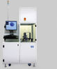
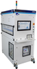
Supplier: Nikon Metrology
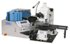
Description: also help prevent damage to wafers. Applications Wafers Benefits & features Remote Access Tool The loader is equipped with a Web server function. When the loader is connected to a LAN, you can create inspection recipes on a PC and easily backup data from the
- Maximum Wafer / Part Size: 200 mm
- Measurements: Defects / ADC
- Mounting / Loading: Floor Mounted / Stand-alone
- Features: Non-contact, Non-destructive, Other
-
Supplier: 3X Ceramic Parts Company Limited
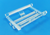
Description: High Precision Zirconia Ceramic Wafer Support Loader Zirconia Ceramic Wafer Carrier Support is highly precision machinind by flapping machine and CNC machined . It is used on the photovaltaic equipment machine to carry the wafer in semiconductor industry . Zirconia
- Density: 6.019996200615109 g/cc
- Thermal Conductivity: 2 W/m-K
- MOR / Flexural Strength: 174,044.2072286364 psi
- Compressive / Crushing Strength: 362,592.0983929925 psi
-
Supplier: MicroSense, LLC
Description: SECS/GEM communication. Automated calibration. Options Wafer prealigner HISCAN for Roughness and structures measurement Applications QA and QC of small size wafers, SiC, Sapphire, Glass, InP, etc…
- Maximum Wafer / Part Size: 50 to 100 mm
- Mounting / Loading: Manual Loading
- Form Factor: Monitor / Instrument
- Technology: Optical / Imaging System
-
-
Supplier: MTI Instruments Inc.
Description: sori, site and global flatness. User-defined and ASTM/SEMI compliant scan patterns are used to generate full 3-dimensional (3D) wafer images. Customized data reports are available for viewing tabular data of each wafer measured with quick, easy export to your spreadsheet program.
- Maximum Wafer / Part Size: 300.00000000000006 mm
- Measurements: Area Mapping, Roughness / Waviness, Shape / Flatness, Thickness - Wafer / Disc (TTV)
- Technology: Capacitance / EM Gage
- Mounting / Loading: Manual Loading
-
Supplier: SemiProbe
Description: SemiProbe IRIS inspection systems inspect, locate and identify defects created during wafer manufacturing, probing, bumping, dicing or general handling, providing microelectronic device manufacturers with accurate, timely quality assurance and process information. The IRIS inspection system
- Measurements: Area Mapping, Defects / ADC, Electrical Test - Parametric / In-line, Particle Contamination
- Mounting / Loading: Manual Loading
- Technology: Optical / Imaging System
- Applications: Semiconductor Wafers
-
Supplier: JST Manufacturing, Inc.
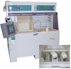
Description: JST's Single Wafer Etching and Stripping System utilizes an automated chemical spray process on a single wafer. The system includes oscillating spray nozzles, adjustable wafer speed (RPM) and precision adjustment of the distance between the nozzles and the surface of the
-
Supplier: Filmetrics, Inc.
Description: Product-Wafer Metrology Made Affordable Process engineers want film thickness measurements fast and without a lot of hassle. Our innovative Thickness Imaging™ technology allows Filmetrics to offer easy recipe set up and industry-leading throughput, at a mere fraction of the cost of competing
- Measurements: Area Mapping
- Applications: CVD / PVD Films, Semiconductor Wafers
- Mounting / Loading: In-situ / System Mounted
- Form Factor: Monitor / Instrument
-
Supplier: Robuster Quartz
Description: Quartz boat is a loader which can be inserted by silicon wafer. So it is applied in semiconductor area. The cleaning process for quartz boat is very strictly. The boat should be dipped in concentration of 4-5% HF solutions keeped for 4 hours. Then soaked in DI water for 1 hours. Quartz
- Shape / Form: Fabricated / Custom Shape
- Glass Type: Quartz
- Features: Specialty / Other
-
Supplier: 3X Ceramic Parts Company Limited
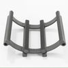
Description: system DOA equipment integrated wafer loading & unloading, unloading the wafers from the Ceramic boat to the cassette or loading the wafers from the cassette to the ceramic boat. Available for double back-to-back wafers in one slot which realize single side diffusion or
- Density: 5.99999621323765 g/cc
- Thermal Conductivity: 2.5 W/m-K
- MOR / Flexural Strength: 116,029.4714857576 psi
- Compressive / Crushing Strength: 290,073.678714394 psi
-
Supplier: 3X Ceramic Parts Company Limited
Description: φ150mm ) silicone wafer , thickness 675 um . They want this part in 99% alumina ceramic . We don’t have the standard wafer boats for customer wafer size , but we custom made it . Before this projects , we have made a 99% alumina horizontal wafer boat , it is for
- Material Type: Carbide Materials, Silicon Carbide
- Shape / Form: Fabricated / Custom Shape
-
Supplier: Locon Sensor Systems, Inc.
Description: Capacitive Miniature Proximity Sensors - WAFER HOUSING The wafer design is basically the size of a thick coin, a great solution for applications where sensor body length is a concern. Housing sizes of 18mm, 22mm, and 30mm Sensing distances from 4mm to 10mm Sometimes the smallest
- Operating Distance: 0.1574804 to 0.393701 inch
- Operating Temperature: -22 to 176 F
- Output Load: 3-Wire NPN, 3-Wire PNP, DC Load
- Sensor Technology: Capacitive Proximity Sensor
-
Supplier: TSI Incorporated
Description: of substrates to be deposited including 150 mm, 200 mm, and 300 mm wafers, supporting of all of your wafer metrology applications and improving product yield.
- Maximum Wafer / Part Size: 150.00000000000003 to 300.00000000000006 mm
- Applications: CVD / PVD Films, Semiconductor Wafers
- Mounting / Loading: Manual Loading
- Features: Other
-
Supplier: TSI Incorporated
Description: of substrates to be deposited including 150 mm, 200 mm, and 300 mm wafers, supporting of all of your wafer metrology applications and improving product yield.
- Maximum Wafer / Part Size: 150.00000000000003 to 300.00000000000006 mm
- Applications: CVD / PVD Films, Semiconductor Wafers
- Mounting / Loading: Manual Loading
- Features: Other
-
Supplier: Prior Scientific, Inc.
Description: automatically moves to the correct load position and activates the loader switch, notifying the loader that the shuttle's wafer chuck is in position to receive the wafer. After the wafer is transferred to the shuttle, the system senses the vacuum change and
- Maximum X-Distance: 154 to 256 mm
- Maximum Y-Distance: 154 to 215 mm
- Minimum Step Size (Resolution): 0.04 µm
- Stage Type: Motorized Stage
-
Supplier: JST Manufacturing, Inc.
Description: Whether processing 6", 8", or 12" wafers or a combination, JST can design an automated wet process tool to meet your needs. Multiple platforms are available as well as a combination acid and/or solvent tool.Multitasking is based on look ahead scheduling to ensure optimal throughput. Just load
-
Supplier: Baumer Ltd.
Description: Baumer’s innovative photoelectric sensors have been successfully employed for years in numerous industrial fields, where they can securely solve even the trickiest detection and measurement problems. A wide variety of employed sensor technologies forms the basis for an extremely broad area of
- Operating Distance: 4.8425223 to 5.6299243 inch
- Operating Temperature: 23 to 122 F
- Output Load: DC Load
- Optical Technology Type: Diffuse
-
Supplier: Jiangyin Deli Laser Solutions Co., Ltd.
Description: Fast scribing speeds; High throughput; High-quality processing results; Significant improvements in yield rates; No consumables; Greatly reduces operating costs. Laser type: DPSS picosecond laser (532nm & 1064nm) Laser power: ≥1W Cooling method: Closed-loop water cooling X-axis: 300mm travel
- X-axis Travel / Length Capacity: 11.81103 inch
- Y-axis Travel / Width Capacity: 11.023628 inch
- Z-axis / Vertical Travel: 0.1968505 inch
- Laser Output Power: 0 to 1 watts
-
Supplier: Armstrong International
Description: TC-300 Series Thermostatic Wafer Steam Trap Carbon Steel For pressures to 250 psig (17 bar) . . . Cold water start-up capacities to 1,000 lb/hr (454 kg/hr) The TC-300 is sized precisely to handle the extremely low condensate load found in most instrument steam tracer lines. The TC-300 traps
- Maximum Operating Pressure: 250 psi
- Maximum Capacity: 1,000.000000000002 lbs/hr
- Size of Connection: 0.75 inch
- Type: Flanged, Socket Weld / Tube, Threaded
-
Supplier: TSI Incorporated
Description: This fully automated particle deposition system deposits PSL and SiO2 spheres as small as 20 nm. Calibrate and qualify your defect inspection tools with ease, confidence, and efficiency by producing high volumes of high-quality custom 300 mm and 200 mm calibration standards. Robotic wafer
- Maximum Wafer / Part Size: 200 to 300.00000000000006 mm
- Applications: CVD / PVD Films, Semiconductor Wafers
- Mounting / Loading: Floor Mounted / Stand-alone
- Features: Other
-
Supplier: TSI Incorporated
Description: This fully automated particle deposition system deposits PSL and SiO2 spheres as small as 10 nm. Calibrate and qualify your defect inspection tools with ease, confidence, and efficiency by producing high volumes of high-quality custom 300 mm and 200 mm calibration standards. Robotic wafer
- Maximum Wafer / Part Size: 200 to 300.00000000000006 mm
- Applications: CVD / PVD Films, Semiconductor Wafers
- Mounting / Loading: Floor Mounted / Stand-alone
- Features: Other
-
Supplier: Nanotronics Imaging
Description: The Nanotronics Imaging nSpec® is an inspection device designed for high resolution microscopy and detection of wafer defects. With particular application in silicon carbide and Galium Nitride epi wafers, the nSpec® offers fast quantification and qualification of defects with detailed
- Measurements: Defects / ADC
- Mounting / Loading: Manual Loading
- Technology: Optical / Imaging System
- Applications: Semiconductor Wafers
-
Supplier: Schmalz Inc.
Description: Wafer gripper for extreme fast, reliable, precise and gentle handling of wet wafers in wet bench applications Handling of wafers after etching and cleaning processes Loading and unloading of conveyor belts Fully or partially automated production of silicon wafers with
-
Supplier: Schmalz Inc.
Description: Wafer gripper for extreme fast, reliable, precise and gentle handling of wet wafers in wet bench applications Handling of wafers after etching and cleaning processes Loading and unloading of conveyor belts Fully or partially automated production of silicon wafers with
-
Supplier: SemiProbe
Description: Manual Prober for contacting of active devices on both sides of the wafer. Precision controls enable the user to probe from the top side of the wafer, the bottom side of the wafer, or to simultaneously probe the top and bottom sides of the wafer.
- Maximum Wafer / Part Size: 100 to 200 mm
- Measurements: Area Mapping, Electrical Test - Parametric / In-line
- Mounting / Loading: Manual Loading
- Technology: Optical / Imaging System
-
Supplier: PI (Physik Instrumente) L.P.
Description: Semiconductor manufacturing: Wafer processing and inspection. Laser machining: Laser welding. Highly dynamic applications in precision automation, smooth scan motion, minimum tracking errors, and short settling times.
- Stroke or X-Axis Travel: 24.015761 to 32.0078913 inch
-
Supplier: MTI Instruments Inc.
Description: The Proforma 300i wafer thickness gage is a capacitance based, differential measurement system that performs non-contact thickness measurements of semiconducting and semi-insulating wafers. By utilizing MTI Push/Pull technology, the Proforma 300i does not require the wafers to
- Maximum Wafer / Part Size: 76 to 300.00000000000006 mm
- Measurements: Area Mapping, Roughness / Waviness, Shape / Flatness, Thickness - Wafer / Disc (TTV)
- Technology: Capacitance / EM Gage
- Mounting / Loading: Manual Loading
-
Supplier: SemiProbe
Description: mm system that meets their precise specifications and requirements. The Probe System for Life (PS4L) family of wafer probing systems is designed based on SemiProbe's patented adaptive architecture. Unlike traditional probe systems, all foundation modules - bases, stages, chucks, microscope
- Maximum Wafer / Part Size: 150.00000000000003 mm
- Measurements: Electrical Test - Parametric / In-line
- Mounting / Loading: Manual Loading
- Technology: Optical / Imaging System
-
Supplier: Schmalz Inc.
Description: Wafer gripper for extremely fast and gentle handling of wafers and solar cells in the production processes Loading and unloading from stacks and conveyor belts Exact positioning during the visual inspection and position measurement allow for on-the-fly breakage detection during the
-
Supplier: Schmalz Inc.
Description: Wafer gripper for extremely fast and gentle handling of wafers and solar cells in the production processes Loading and unloading from stacks and conveyor belts Exact positioning during the visual inspection and position measurement allow for on-the-fly breakage detection during the
-
Supplier: Newport MKS
Description: temperatures in the 10–100 Hz frequency range. This level of damping is two to five times better than other commercial elastomers. The high damping factor makes them ideal for supporting and damping the high acceleration amplitudes produced by very high throughput stages used in wafer
- Maximum Load Capacity (Per mount): 1,323 lbs
- Height or Thickness (Before loading): 3.63 inch
-
Supplier: Newport MKS
Description: the 10–100 Hz frequency range. This level of damping is two to five times better than other commercial elastomers. The high damping factor makes them ideal for supporting and damping the high acceleration amplitudes produced by very high throughput stages used in wafer positioning, inspection
- Maximum Load Capacity (Per mount): 882 lbs
- Height or Thickness (Before loading): 3.63 inch
-
Supplier: Newport MKS
Description: the 10–100 Hz frequency range. This level of damping is two to five times better than other commercial elastomers. The high damping factor makes them ideal for supporting and damping the high acceleration amplitudes produced by very high throughput stages used in wafer positioning, inspection
- Maximum Load Capacity (Per mount): 1,764 lbs
- Height or Thickness (Before loading): 3.63 inch
-
Supplier: Skyworks Solutions, Inc.
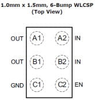
Description: over-temperature protection and recovers automatically when the fault is removed. The SKY84632 is available in a 6-bump, 1.0mm x 1.5mm, Wafer-Level Chip-Scale Package (WLCSP) and is rated over the -40°C to +85°C temperature range.
- Features: Other
- Package Type: Surface Mount










Find Suppliers by Category Top
Featured Products Top
-
 Product Overview Used in semiconductor wafer transfer robots, sorters, and load ports for picking, placing, and transferring wafers between process modules and FOUPs. Fountyl ceramic end effectors are manufactured from high-purity alumina (Al2O3 99 (read more)
Browse Industrial Ceramic Materials Datasheets for Fountyl Technologies Pte. Ltd. -
Tokyo Electron’s Prexa™ MS is a fully automated 300mm wafer prober designed for advanced DRAM testing. As memory devices become more complex—requiring more test pins, generating more heat, and demanding precise high-load control—the system needs highly reliable data (read more)
Browse Network Switches Datasheets for Volktek Corporation -
High-Precision Alumina Ceramic End Effector Tailored for Semiconductor Wafer Handling This end effector is made from premium alumina ceramic, combining exceptional wear and (read more)
Browse Aluminum Oxide and Alumina Ceramics Datasheets for Fountyl Technologies Pte. Ltd. -
Uniform permeability and strong adsorption ensure silicon wafers are firmly held without slipping during grinding, improving process stability. Dense (read more)
Browse Wafer Chucks Datasheets for Fountyl Technologies Pte. Ltd. -
Supports ultra-precision wafer transport and alignment Ensures stable trajectory control during exposure processes Enables loading, alignment (read more)
Browse Silicon Carbide and Silicon Carbide Ceramics Datasheets for Fountyl Technologies Pte. Ltd. -
, ensuring non-contact, damage-free handling of wafers, panels, and thin substrates. Typical Applications Semiconductor vacuum chuck systems ( Wafer grinding vacuum chuck \ Wafer dicing vacuum chuck \ Printing vacuum chuck) Cleaning the vacuum chuck (read more)
Browse Aluminum Oxide and Alumina Ceramics Datasheets for Xiamen Innovacera Advanced Materials Co., Ltd. -
Maury automated tuners are precision instruments optimized for in-fixture and on-wafer, RF/microwave test and measurement applications. They are ideal for automated or manual application where the need is to match the impedance of a microwave circuit element, or to establish specific impedances (read more)
Browse Dimensional Gages and Instruments Datasheets for Maury Microwave -
Product Overview Used in semiconductor wafer transfer robots, sorters, and inspection equipment for handling wafers in cleanroom and vacuum environments. Fountyl ceramic end effectors are manufactured from high-purity alumina (Al2O3 99.5%) and silicon carbide (SiC 99 (read more)
Browse Industrial Ceramic Materials Datasheets for Fountyl Technologies Pte. Ltd. -
-current wafer processing systems, precision sensor feedthroughs, or fiber optic monitoring in load locks, our assemblies are built for reliability in the most demanding semiconductor environments. (read more)
Browse Feedthroughs Datasheets for Douglas Electrical Components -
heavy kinematic loads. Ultra-Cleanroom Compatibility: Due to inherent material density and surface stability, these guide rails minimize operational particle generation, eliminating contamination risks inside high-vacuum cleanrooms. Total Chemical (read more)
Browse Aluminum Oxide and Alumina Ceramics Datasheets for Fountyl Technologies Pte. Ltd.
Conduct Research Top
-
EETimes.com | Electronics Industry News for EEs & Engineering Managers
Slew of high-tech execs on Santa's naughty list Just days before Santa loads up the sleigh the make his famous trek, the U.S. Justice Department has provided a reminder that many high-tech executives had better be prepared to find lumps of coal in their stockings on Christmas morning. SED's CES
-
EETimes.com | Electronics Industry News for EEs & Engineering Managers
Slew of high-tech execs on Santa's naughty list Just days before Santa loads up the sleigh the make his famous trek, the U.S. Justice Department has provided a reminder that many high-tech executives had better be prepared to find lumps of coal in their stockings on Christmas morning. Commentary
-
EETimes.com | Electronics Industry News for EEs & Engineering Managers
Heard on the Beat (Nov. 30) Heard on the Beat, Nov. 30 TEL enhances prober to handle mix of 200- and 300-mm wafers TOKYO -- In a move to increase flexibility and throughput in wafer-test operations, Tokyo Electron Ltd. today announced an enhanced version of its P-12XL prober, which adds a new sort
-
Factors to Consider When Choosing a Crossed Roller Bearing (.pdf)
it's wafer positioning for the efficient manufacture of ICs, pick and place, vision inspection, parts transfer, a microscope stage under computer control or precise vertical movements, linear bearings have had to evolve rapidly in order to carry heavier loads, take up less space and be reliably precise.
More Information Top
 Indicates content that may require registration and/or purchase.

-
An automated loading and unloading system for a maglev wafer transport path
The design specifications for an automated wafer loader -un- loader are partially dictated by standard mechanical design prac- tices and partially result from the unique needs of silicon process- ing.
-
High Throughput And Accuracy X-Ray Stepper With Plasma Source
three -channel pre- and fine alignment optical system, coarse and fine stages, an automatic wafer loader and the aligner controller with a minicomputer.
-
One small step: world's first integrated EUVL process line
A dedicated vacuum control rack is used to monitor and control the vacuum levels in the source, projection optics, reticle stage, wafer loader , and main chamber.
-
Flare evaluation for 32-nm half pitch using SFET
Wafer loader .
-
Low Voltage Sem Metrology For Pilot Line Applications
SEM 1, used in a production pilot line facility, has an automated cassette -to- cassette wafer loader and can only observe samples at normal beam incidence.
-
Measurement And Inspection Of Contact Holes On In-Process Vlsi Devices With A Low. Voltage Scanning Electron Microscope (Sem)
Automatic Wafer Loader .
-
Total performance of Nikon EB stepper R&D tool
Wafer Loader Station Load Lock Loader .
-
Nikon EUVL development progress update
Nikon has completed almost all module fabrication such as full-field projection optics module, illumination optics module, vacuum body module, vacuum compatible reticle/wafer stage modules, reticle/ wafer loader modules, and EUV light source module.
-
Manufacturing technique for robust and modular smart composites
Wafer Loader .
-
Nikon EPL tool development summary
In addition to the electron optics and the stages, there are wafer loader and reticle loader subsystems and vacuum pumps and its components.