Digital Integrated Circuit Design

Working from the fundamentals of transistor-level design and building up to system-level considerations, this text demonstrates how to design state-of-the-art high performance digital integrated circuits.
The circuit diagrams, netlist files, and output data associated with SPICE simulations of selected examples are presented in this section. The device models, unless explicitly present in the netlist file, are assumed to be as given in Section 2.4, where SPICE-modeling parameters are discussed.
The circuit diagram of Example 3.6 is shown in Fig. 3.52. Node labels correspond to those used in the input netlist below. The reverse-biased diode is modeled with a junction potential of 0.9 V and a total junction capacitance of 0.002 pF for a 0 V applied voltage. The remaining diode parameters assume their default values (refer to the SPICE manuals for default parameter values specific to the release of SPICE in use).
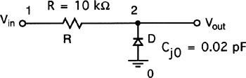
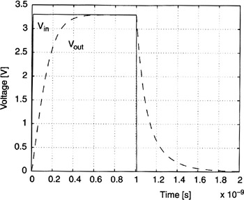
The transient response of charging and discharging a diode*R 1 2 10kD 0 2 DMOD*VIN 1 0 PULSE (0 3.3 0p 10p 10p 0.99n 2.0n)*.MODEL DMOD D (CJ0 = 0.02e-12, PB = 0.9)*.OPTION NOMOD POST INGOLD = 2 NUMDGT = 6 BRIEF.TRAN 0.01n 2.0n.PRINT TRAN V(1) V(2).END
The transient response of the simulation is plotted in Fig. 3.53. The respective rise and fall times are t +70% = 0.16 ns and t ?70% = 0.13 ns, which compare favorably to the previous calculations, which yielded 0.17 and 0.13 ns, respectively.
The circuit required to...