Digital Integrated Circuit Design

Working from the fundamentals of transistor-level design and building up to system-level considerations, this text demonstrates how to design state-of-the-art high performance digital integrated circuits.
As a useful aid, all of the equations for the large-signal and small-signal modeling of diodes, MOS transistors, and bipolar transistors, along with values for the various constants, are listed in the next few pages.
Constants
| q = 1.602 10 ?19 C | k = 1.38 10 ?23 J K ?1 |
| n i = 1.1 10 16 carriers/m 3 at T = 300 K | ? 0 = 8.854 10 ?12 F/m |
| K ox ? 3.9 | K s ? 11.8 |
| ? n = 0.05 m 2/V s | ? p = 0.02 m 2/V s |
Diode Equations
| Reverse-Biased Diode (Abrupt Junction) | |
|---|---|
| | |
| | |
| |
Forward-Biased Diode
| I D = I Se V D/V T | |
| |
Small-Signal Model of Forward-Biased Diode
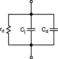
| | C T = C d + C j |
| | C j ? 2C j0 |
|
|
The following equations are for n-channel devices; for p-channel devices, put negative signs in front of all voltages. These equations do not account for short-channel effects (i.e., L < 2L min).
Triode Region ( V GS > v tn, V DS ? V eff)
| | |
| V eff = V GS ? V tn | |
| | |
| |
Small-Signal Model in Triode Region (for V DS << V eff)
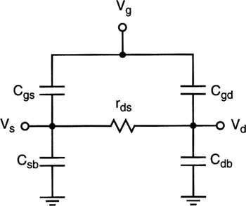
| | |
| | |
Active (or Pinch-Off) Region ( V GS > V tn,