Fundamentals of Carrier Transport, Second Edition

Including many homework exercises and a variety of worked examples, this book is an accessible introduction to the behavior of charged carriers in semiconductors and semiconductor devices.
Until recently, a deep understanding of electron transport in semiconductor devices has not been essential to the device engineer because the familiar drift-diffusion equation,
| (0.1) | |
described devices well, and the transport parameters, n and D n did not need to be computed from first principles because they had been carefully measured. For advanced devices, however, the situation is much different. In small devices, n and D n are no longer material- and field-dependent parameters; they depend on microscopic physics, on the structure of the device, and even on the applied bias. A variety of materials is now being investigated, and with modern epitaxial technology it is even possible to engineer material properties. This book begins at the microscopic level and progresses towards the macroscopic level of devices.
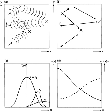
At the most basic level, electrons in semiconductors are quantum mechanical waves propagating through the device under the influence of the crystal, applied, and scattering potentials as indicated in Fig. 0.1a. Chapter 1 begins at this level and shows that when the scale of the device is large enough, the electron can be treated much as a classical particle as indicated in Fig. 0.1b. Electron scattering, however, is the result of short-range forces and must be treated quantum mechanically. Calculation of scattering probabilities per unit time for the perturbing potentials encountered in common semiconductors is the subject of Chapter 2.