Microchip Fabrication: A Practical Guide to Semiconductor Processing, Fifth Edition
This chapter will introduce the four basic processes used in the wafer fabrication to form the electrical elements of an integrated circuit in and on the wafer surface. Circuit design is traced from the functional diagram to the production of photomasks and reticles. Wafer and chip features and terminology are detailed. Finally, a flow diagram for the fabrication of a simple semiconductor device is presented.
Upon completion of this chapter, you should be able to:
Identify and explain the four basic wafer operations.
Identify the parts of a wafer.
Draw a flow diagram of the circuit-design process.
Explain the definition and use of a composite drawing and mask set.
Draw cross sections showing the doping sequence of basic operations.
Draw cross sections showing the metallization sequence of basic operations.
Draw cross sections showing the passivation sequence of basic operations.
Identify the parts of an integrated circuit chip.
The four stages of microchip manufacturing are materials preparation, crystal growth and wafer preparation, wafer fabrication, and packaging. The first two stages have been explored in Chapter 3. In this chapter, the fundamentals of stage 3, wafer fabrication, are explained.
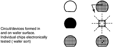
Wafer fabrication is the manufacturing processes used to create the semiconductor devices in and on the wafer surface. The polished starting wafers come into fabrication with blank surfaces and exit with the surface covered with hundreds of completed chips (Fig. 4.1).