Power Amplifier Design: A Collection from Applied Microwave & Wireless

With contributions from more than 20 experts, these articles present valuable resources for power amplifier linarization, measuring, modeling and distortion.
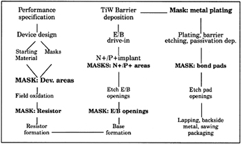
Figure 5 shows a schematic cross-section for the device structure in use for up to 1 GHz. A typical interdigitated cell layout was shown in Figure 4, with the position of the cross-section in Figure 5 marked with an arrow. Common silicon planar technology is used. A principle design and process flow is shown in Figure 6.
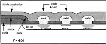
At high current levels, only the periphery of the emitter areas is delivering power because of the current crowding effect. The emitter perimeter is therefore made very large and the fingers very narrow. The base contact fingers are placed between the emitters, thus reducing the extrinsic base resistance from the base contact to the emitter edge, to increase RF gain. The metallization extends on top of the emitter and base contact areas. Very little parasitic resistance is added compared to other layout principles.
There is no interdevice isolation; the whole silicon substrate is the collector, which means that no circuit functions can be designed using a single chip in this technology. Emitter and base are contacted using the front side bond pads.
There are various methods to obtain high breakdown voltage at the device edges. For Ericsson s 1 GHz technology, a classical method with three floating depletion rings is used. The rings have the same doping as the base region but are not...