Power Amplifier Design: A Collection from Applied Microwave & Wireless

With contributions from more than 20 experts, these articles present valuable resources for power amplifier linarization, measuring, modeling and distortion.
Bias choices determine linearity, gain and efficiency, but also require attention to thermal effects
By Cindy Blair
From APPLIED MICROWAVE & WIRELESS, VOL. 12, NO. 1, JANUARY 2000
The code division multiple access (CDMA) and wideband CDMA (WCDMA) wireless standards have dramatically impacted the optimization criteria that a wireless base station designer might choose in designing or selecting RF Power amplifiers. Now, more than ever before, linearity is of paramount importance. Lateral DMOS devices have provided superior performance at a reasonable price per watt. RF power amplifier designers must choose the bias point that will give them the best trade-offs between linearity, gain and efficiency. To provide these high degrees of linearity under all reasonable conditions, this bias point must be reasonably maintained over time and temperature.
A FET device has three parameters that change with increasing temperature: the gate threshold shifts, g m drops, and R DS (on) goes down. The combined result of this is shown in Figure 1, displaying a standard typical temperature plot given by most manufacturers of commercial LDMOS devices. The gate bias values shown are normalized to 1 volt at 25 degrees Celsius and depict the bias values needed to maintain the graphed current point over temperature.
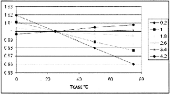
At low drain currents, the LDMOS device has a positive temperature coefficient. As the drain current increases, the positive coefficient becomes progressively less positive, until at very high...