Power Amplifier Design: A Collection from Applied Microwave & Wireless

With contributions from more than 20 experts, these articles present valuable resources for power amplifier linarization, measuring, modeling and distortion.
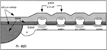
As the demands for higher operating frequencies have grown, a structure similar to Figure 7 has been taken in use for PDC (1500 MHz), PCS (1900 MHz) and so on and for new frequency bands above 2 GHz.
To reduce parasitic capacitance from the metallization to the substrate (mainly collector-base capacitance) to sustain RF gain, the thickness of the field oxide isolation has been increased from around one micron to at least three microns.
Such a thick isolation can be achieved by increasing the initial thermally grown oxide or depositing a thick isolation layer, and then an etch to open the device areas; or use a LOCOS isolation, similar to a CMOS device but with much larger oxide thickness.
However, to open the small emitter/base contacts and metalize the narrow openings successfully, it is necessary to reduce the topology. Various forms of fully recessed local oxidation can be applied with an almost planar structure as a result. The recessed structure is obtained by depositing a nitride/oxide layer, as for a LOCOS structure. The nitride/oxide is then etched away outside the device areas. The etching is continued up to one micron into the silicon substrate. After a long oxidation, which can be accelerated by the use of high-pressure oxidation (HIPOX), the almost perfectly planar structure in Figure 7 is obtained.
To further reduce parasitic R and C to increase gain, the pitch has been scaled...