Practical MMIC Design

Filled with real-world design techniques and rules of thumb, this practical resource offers professionals a unique look into the day-to-day practices of MMIC production and the economics associated with it.
|
| 2.1 What characteristics of the semiconductor material determine the frequency range over which it can be used for producing MMICs? |
|
|
| 2.2 Which semiconductor substrate materials exhibit a wide band-gap, making them suitable for high-output power applications? |
|
|
| 2.3 What are the typical gate voltage and drain current bias settings for a GaAs MESFET? |
|
|
| 2.4 What is the bias voltage required between the base and emitter contacts of a typical silicon bipolar transistor to overcome the built-in junction potential and switch the transistor fully on? |
|
|
| 2.5 Why must the electrical connections between components on an MMIC be treated as transmission lines? |
|
|
| 2.6 How does the characteristic impedance of a microstrip transmission line vary as the width of the track is increased, and is this due to the track looking more inductive or capacitive? |
|
|
| 2.7 Figure 2.36 shows the section and plan view of a nichrome resistor. If the nichrome film has a resistivity of 50 ?/square, what is the resistance of this resistor? 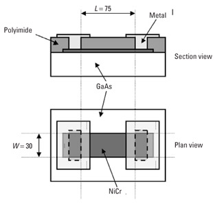 Figure 2.36: Section and plan view of a thin-film nichrome resistor. |
|
|
| 2.8 Figure 2.37 shows the section and plan view of polyimide and silicon nitride MIM capacitors. Given that the silicon nitride has a thickness of 1,200 and a dielectric constant of ? = 7 x 10 -11 and the polyimide thickness is 1.5, ? m and has a dielectric constant of ? = 3.6 x 10 -11, what is the capacitance of... |