Electrical Properties Of Materials, Seventh Edition
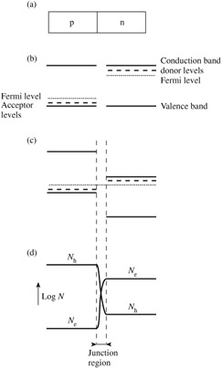
Not unexpectedly, when we want to produce a device, we have to put things together. This is how we get the simplest semiconductor device the p-n junction, which consists of a p- and an n-type material in contact [Fig. 9.1(a)]. Let us imagine now that we literally put the two pieces together. [1] What happens when they come into contact? Remember, in the n-type material there are lots of electrons, and holes abound in the p-type material. At the moment of contact the electrons will rush over into the p-type material and the holes into the n-type material. The reason is, of course, diffusion: both carriers make an attempt to occupy uniformly the space available. Some electrons, moving towards the left, collide head-on with the onrushing holes and recombine, but others will be able to penetrate farther into the p-type material. How far? Not very far; or, to put it another way, not many get very far because their efforts are frustrated by the appearance of an electric field. The electrons leave positively charged donor atoms behind, and similarly there are negatively charged acceptor atoms left in the p-type material when the holes move out. This charge imbalance will give rise to an electric field, which will increase until equilibrium is reached.