Electrical Properties Of Materials, Seventh Edition

9.5: Junction Capacity

9.5 Junction Capacity

I would like to say a few more words about the reverse biased junction. Its most interesting property (besides the high resistance) is that the presence of two layers of space charge in the depletion region makes it look like a capacitor.

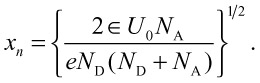
We may calculate its capacitance in the following way. We first derive the relationship between the width of the depletion layer in the n-region and the voltage in the junction, which may be obtained from equations (9.2) and (9.8). We get

(9.18)

U 0 is the 'built-in' voltage.

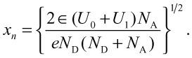
For reverse bias the only difference is that the barrier becomes larger, that is U 0 should be replaced by U 0 + U 1, yielding

(9.19)

U 1 is the applied voltage in the reverse direction.

The total charge of the donor atoms is

(9.20)

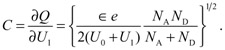
Now a small increase in voltage will add charges at the boundary as it happens in a real capacitance. We may, therefore, define the capacitance of the junction (per unit area) as

(9.21)

We can now assign an equivalent circuit to the junction and attribute a physical function to the three elements (Fig. 9.8). R 1 is simply the ohmic resistance of the 'normal'that is not depleted, semiconductor. R( U 1) is the junction resistance. It is very small in the forward direction (0.1 + 10 ? typically) and large in the reverse direction (10 6 - 10 8 ? typically).

UNLIMITED FREE
ACCESS
TO THE WORLD'S BEST IDEAS

SUBMIT
Already a GlobalSpec user? Log in.

This is embarrasing...

An error occurred while processing the form. Please try again in a few minutes.

Customize Your GlobalSpec Experience

Category: Diodes
Finish!
Privacy Policy

This is embarrasing...

An error occurred while processing the form. Please try again in a few minutes.