Failure Analysis of Engineering Materials

This text introduces the important aspects associated with the failure analysis of engineering components, and provides a treatment of both macroscopic and microscopic observations of fracture surfaces.
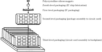
The term packaging of electronic components implies several levels of packaging, which can be summarized as
Zeroth-level packaging including semiconductors, attachment materials, and substrate materials.
First-level packaging of chips onto single-chip modules (SCMs) or multichip modules (MCMs) involving wire interconnects, tape interconnects, case materials, lid seals, and leads.
Second-level packaging of SCMs, MCMs, connectors, etc., onto printed-circuit boards (PCBs) involving reinforcement fiber materials, resins, laminates, flexible printed board materials, and conformal coatings.
Third-level packaging of PCBs, cables, power supplies, ancillary systems, etc., onto a frame or box (e.g., motherboard). From a materials standpoint, this involves backpanel materials, connector materials, cables, and flex circuit materials.
The ultimate objective of packaging is to ensure that all the components of the package operate in concert. Figure 6.76 schematically depicts the four levels of packaging.
At the first level, the chip or IC device is connected to its carrier by wire bonding, flip-chip attachment, tape-automated bonding and z-direction adhesives. In wire bonding, electrical connection between the pads on the chip and the external carriers is made by bonding fine gold or aluminum wires to both pads. In the case of flip-chip technology, the chip is inverted and bonding between chip and the carrier pads is achieved with either solder or gold bumps. Since the advent of organic (polyimide) substrates, the metal used for bonding has had to be modified...