Electronic and Optoelectronic Properties of Semiconductor Structures

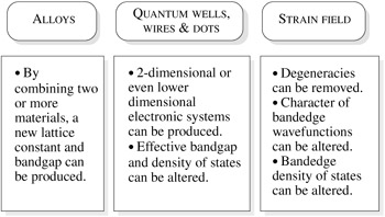
In the previous chapter we have seen how the intrinsic properties of a semiconductor as reflected by its chemical composition and crystalline structure lead to the unique electronic properties of the material. Can the bandstructure of a material be changed? The answer is yes, and the ability to tailor the bandstructure is a powerful tool. Novel devices can be conceived and designed for superior and tailorable performance. Also new physical effects can be observed. In this chapter we will establish the physical concepts which are responsible for bandstructure modifications. There are three widely used approaches for band tailoring (or engineering). These three approaches are shown in Fig. 3.1 and are:
Alloying of two or more semiconductors;
Use of heterostructures to cause quantum confinement; and
Use of built-in strain via lattice mismatched epitaxy.
These three concepts are increasingly being used for improved performance in electronic and optical devices.
The easiest way to alter the electronic properties or to produce a material with new properties is based on making an alloy. Alloying of two materials is one of the oldest techniques to modify properties of materials, not only in semiconductors, but in metals and insulators as well.
The desire to form alloys in semiconductors is motivated by two objectives:
Achieving a desired bandgap. This motivation drives a great deal of alloy studies in the laser/detector area. The bandgap essentially determines the energy of the light emitted and...