Electronic and Optoelectronic Properties of Semiconductor Structures

Incorporation of strain in heterostructures has become an accepted technique to modify bandstructure. A number of important electronic and optoelectronic devices exploit strain in their design. In Chapter 1 and Chapter 3 we have seen how strain epitaxy occurs and how bandstructure is modified by strain. In this Appendix we will establish the basic equations for stress-strain relations and strain energy in a semiconductor. We will address the cubic structure, although similar treatment can be established for other lattices.
In this section we will establish some basic expressions for strain in crystalline materials. We will confine ourselves to small values of strain. In order to define the strain in a system we imagine that we have a set of ortho-normal vectors
,
,
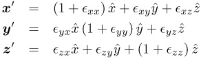
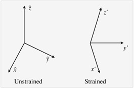
, in the unstrained system. Under the influence of a uniform deformation these axes are distorted to x', y', z', as shown in Fig. A.1. The new axes can be related to the old one by
| (A.1) | |
The coefficients ? ?? define the deformation in the system. The new axes are not orthogonal in general. Let us consider the effect of the deformation on a point r which in the unstrained case is given by
| (A.2) | |
After the distortion the new vector is given by
| (A.3) | |
Note that by definition the coefficients x, y, z of the vector are unchanged. The displacement of...