Electronic and Optoelectronic Properties of Semiconductor Structures

2.3: METALS, INSULATORS, AND SEMICONDUCTORS

2.3 METALS, INSULATORS, AND SEMICONDUCTORS

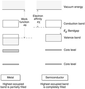
We know from atomic physics that bound electrons have discrete energy levels separated by forbidden energy regions. In solids the discrete levels broaden to form allowed bands which are separated by bandgaps. Once one knows the electronic spectra the important question is: Which of these allowed states are occupied by electrons and which are unoccupied? Two important situations arise when we examine the electron occupation of allowed bands: In one case we have a situation where an allowed band is completely filled with electrons, while the next allowed band is separated in energy by a gap E g and is completely empty at 0 K. In a second case, the highest occupied band is only half full (or partially full). These cases are shown in Fig. 2.3.


Figure 2.3: A schematic description of electron occupation of the bands in a metal and semiconductor (or insulator). In a metal, the highest occupied band at 0 K is partially filled with electrons. Also shown is the metal work function. In a semiconductor at 0 K, the highest occupied band is completely filled with electrons and the next band is completely empty. The separation between the two bands is the bandgap E g. The electron affinity and work function are also shown.

At this point a very important concept needs to be introduced. When an allowed band is completely filled with electrons, the electrons in the band cannot conduct any current. This important concept is...

UNLIMITED FREE
ACCESS
TO THE WORLD'S BEST IDEAS

SUBMIT
Already a GlobalSpec user? Log in.

This is embarrasing...

An error occurred while processing the form. Please try again in a few minutes.

Customize Your GlobalSpec Experience

Category: Semiconducting Materials
Finish!
Privacy Policy

This is embarrasing...

An error occurred while processing the form. Please try again in a few minutes.