Electronic and Optoelectronic Properties of Semiconductor Structures

2.10: MOBILE CARRIERS: INTRINSIC CARRIERS

2.10 MOBILE CARRIERS: INTRINSIC CARRIERS

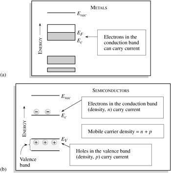
From our brief discussion of metals and semiconductors in Section 2.3, we see that in a metal, current flows because of the electrons present in the highest (partially) filled band. This is shown schematically in Fig. 2.20a. The density of such electrons is very high (~ 10 23 cm -3). In a semiconductor, on the other hand, no current flows if the valence band is filled with electrons and the conduction band is empty of electrons. However, if somehow empty states or holes are created in the valence band by removing electrons, current can flow through the holes. Similarly, if electrons are placed in the conduction band, these electrons can carry current. This is shown schematically in Fig. 2.20b. If the density of electrons in the conduction band is n and that of holes in the valence band is p, the total mobile carrier density is n + p.


Figure 2.20: (a) A schematic showing allowed energy bands in electrons in a metal. The electrons occupying the highest partially occupied band are capable of carrying current. (b) A schematic showing the valence band and conduction band in a typical semiconductor. In semiconductors only electrons in the conduction band and holes in the valence band can carry current.

In Appendix B we discuss the density of states of electrons near bandedges. The density of state N( E) is a very important concept and gives us the number of allowed...

UNLIMITED FREE
ACCESS
TO THE WORLD'S BEST IDEAS

SUBMIT
Already a GlobalSpec user? Log in.

This is embarrasing...

An error occurred while processing the form. Please try again in a few minutes.

Customize Your GlobalSpec Experience

Category: Semiconducting Materials
Finish!
Privacy Policy

This is embarrasing...

An error occurred while processing the form. Please try again in a few minutes.