Electronic and Optoelectronic Properties of Semiconductor Structures

In this Appendix we will review several important experimental techniques that allow us to determine structural, electronic, and optical properties of semiconductor structures. The intent of this review is not to present details on these experimental techniques, but to present the reader with an overview of what their capabilities are and what the difficulties are.
Diffraction experiments are essential tools to determine the structural quality of crystalline materials. These techniques allow one to measure the lattice parameters of crystals and also provide information on structural imperfection. The basis for all diffraction experiments is the Bragg law which in its simplest form is
| (B.1) | |
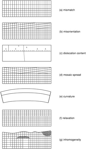
where d is the spacing between identical planes, ? is the wavelength and ? is the diffraction angle. With cleverly designed experiments and sophisticated data analysis this simple equation can form the basis of very detailed structural information. In Figure B.1 we show a schematic of some important pieces of structural information that are obtained from diffraction experiments. Of course, the diffraction experiments also reveal information on lattice constants for bulk semiconductors.
Lattice Mismatch: Growth of epilayers on substrates that have a lattice constant different from the epilayers constant is becoming increasingly important. As discussed in this chapter if the film is relaxed the epilayer will produce a shift ? ? in the diffraction pattern with respect to the substrate.