High Voltage Diodes Information
Last revised: November 1, 2024
Reviewed by: Scott Orlosky, consulting engineer
 High voltage diodes are those that operate at roughly around 2,000 volts and above. There are many types of high-voltage diodes, generally differentiated based on their construction.
Types of Diodes
Here we introduce some of the most important high voltage diodes available. The most commonly specified type of high voltage diodes are PIN, Schottky, and Zener
PIN Diodes PIN diodes are three-layer semiconductor diodes consisting of an intrinsic layer separating heavily-doped P and N layers. The charge stored in the intrinsic layer, in conjunction with other diode parameters, determines the resistance of the diode at RF and microwave frequencies. Typically, this resistance ranges from kilohms to less than 1 ohm for a given diode.
High voltage PIN diodes are often used as switches or attenuator elements. RF diodes are designed to handle frequency (RF) signals in devices such as stereo amplifiers, radio transmitters, television monitors, and other radio frequency or microwave devices.
High Voltage Schottky Diodes — Schottky barrier diodes are used in high frequency and fast-switching applications. In their simplest form, they consist of a metal layer that contacts a semiconducting element. This metal / semiconductor junction acts like a rectifier, allowing current to pass through more readily with one polarity than the other.
Schottky diodes are used primarily in high frequency and fast-switching applications. Because they operate only with majority carriers, there is no reverse leakage current as with other types of diodes.
With Schottky diodes, the metal region is heavily populated with conduction-band electrons. The N-type semiconductor region is lightly doped. When forward-biased, the higher energy electrons in the N-region are injected into the metal region, where they give up their excess energy very rapidly.
Since there are no minority carriers (as with conventional rectifier diodes), there is a very rapid response to a change in bias. For this reason, Schottky diodes are used in high-frequency applications and in many digital circuits to decrease switching times. Schottky diodes are also known as hot-carrier diodes.
PN Junction Diodes — PN junction diodes are designed for general-purpose applications. A high voltage Zener diode is a special type of PN junction diode that is designed to operate in reverse bias (by applying a higher voltage to the N material than to the P material). The Zener diode acts as a normal rectifier until the applied voltage reaches a certain value (the avalanche voltage). At this point the diode conducts producing a large current.
Other high voltage diodes that are available are Transient voltage suppressor diodes (TVS) are semiconductors that limit over-voltages. Current limiting diodes (CLD) regulate current over a wide voltage range. Gunn diodes are transfer electron devices (TED) which exhibit a negative resistance region. Impact ionization avalanche transit-time (IMPATT) diodes are high voltage diodes which operate at a very high frequency and power.
 High Voltage Varactor Diodes — Varactor diodes are P-N junction diodes that act as voltage-controlled capacitors when operated under reverse bias. PN junctions have inherent capacitance. When the junction is reverse biased, increasing the applied voltage causes the depletion region to widen, thus increasing the effective distance between the two "plates" of the capacitor and decreasing the effective capacitance. By adjusting the doping gradient and junction width, the capacitance range can be controlled, and the way-capacitance changes with the applied reverse voltage.
A four-to-one capacitance range is not problematic. In fact, a typical varactor diode (sometimes called a "varicap diode") can vary from 60 picofarads (pf) at zero-bias down to 15 pf at 20 volts (V). Precision manufacturing can achieve a capacitance range of up to ten-to-one. Typically, varactor diodes are used in electronic tuning systems to eliminate the use of and need for moving parts.
High Voltage Diode Performance Specifications
- Repetitive peak reverse voltage, maximum reverse voltage, the maximum allowable voltage, instantaneous value of repetitive reverse voltage.
- Reverse current is the current value when the specified reverse voltage is applied.
- Reverse recovery time is the time needed for the reverse current to reach a specified level when the reverse voltage is applied while the device is conducting in the forward direction.
- Forward voltage is voltage across the diode terminals which results from the flow of current in the forward direction.
- Power dissipation is the amount of power which high voltage diodes dissipate when in the on-state.
- Junction operating temperature is the range of temperatures in which high voltage diodes are designed to operate.
Types of Leads/Connections
 Axial leads extend from the high voltage diode's ends and along its axis.
- Radial leads extend from the diode's sides instead of from its ends.
- Flying leads project horizontally from the high voltage diode.
- Tab leads are terminals designed for direct mounting into a circuit board socket.
- Screw or insert leads are designed to be fastened with screws.
- Gull-wing leads are popular because they are relatively inexpensive to mold and form. They are flexible enough to withstand thermal expansion and contraction. Inspecting the integrity of the gull-wing lead to circuit board solder connection is relatively easy.
- High voltage diodes with J-leads use less board space than gull-wing leads; however, because these lead-to-board solder connections are hidden, they are hard to inspect; they are more difficult to form.
- Diodes that use surface mount technology (SMT) do not have leads. Instead, they are pad-mounted.
High Voltage Diodes FAQs
What are the fabrication techniques for high voltage PN junctions?
The planar junction fabrication technique involves creating a flat junction. The deep-diffused junction fabrication technique involves creating a junction with severe angles, often resulting in a "mesa" appearance.
How do you test VF and polarity in high voltage diodes?
To test the forward voltage (VF) and polarity in high voltage diodes, you can follow these steps:
- Set up the multimeter: Use a digital multimeter (DMM) capable of measuring diode forward voltage.
- Set the multimeter to the diode test mode. Connect the probes: Connect the positive (red) probe to the anode of the diode. Connect the negative (black) probe to the cathode of the diode.
- Measure the forward voltage: The multimeter will apply a small forward voltage to the diode and measure the voltage drop across it.
- The displayed value is the forward voltage (VF) of the diode.
Testing Polarity
- Set up the multimeter: Use a digital multimeter (DMM) set to the diode test mode.
- Identify the anode and cathode: Connect the positive (red) probe to one terminal of the diode. Connect the negative (black) probe to the other terminal.
- Check the reading: If the multimeter shows a low voltage drop (typically 0.7 V for silicon diodes), the positive probe is connected to the anode and the negative probe to the cathode. If the multimeter shows an open circuit or a very high voltage drop, reverse the probes. The correct polarity is when the multimeter shows a low voltage drop.
What are the advantages of using deep-diffused junction fabrication for high voltage diodes?
The advantages of using deep-diffused junction fabrication for high voltage diodes can be understood by examining the specific characteristics and benefits of this technique. Here are the key advantages:
Structural Benefits
Deep-diffused junctions often have severe angles, creating a "mesa" appearance. This structure can enhance the electrical characteristics of the diode by providing better control over the junction properties.
The use of an epitaxial layer in deep-diffused junctions can improve the overall quality and performance of the diode. This layer can help in achieving a more uniform doping profile and better electrical characteristics.
Performance Enhancements
Deep-diffused junctions are particularly suitable for high voltage applications. The structure allows for better distribution of the electric field, reducing the likelihood of breakdown and improving the diode's ability to handle high voltages.
The robust structure of deep-diffused junctions can lead to improved reliability and longevity of the diode. This is particularly important in applications where the diode is subjected to high stress and harsh operating conditions.
Fabrication Flexibility
It allows for the use of a variety of dopants, providing flexibility in tailoring the diode's electrical characteristics to specific application requirements.
The technique facilitates the customization of the junction properties, enabling the creation of diodes with specific performance characteristics suited to particular applications.
Deep-diffusion junctions brings advantages to high voltage diodes, including structural benefits, enhanced performance, and fabrication flexibility. These advantages make deep-diffused junctions particularly suitable for high voltage applications where reliability and performance are critical.
What are the characteristics of planar fabrication techniques?
Planar Junction Fabrication
Planar junctions are created using a flat junction structure. The process involves diffusing dopants into a flat silicon wafer to form the PN junction. The fabrication process typically involves photolithography and diffusion processes to create the junction. The surface of the wafer is passivated to protect the junction and improve performance.
Planar junctions are easier to manufacture and are suitable for high-volume production. They offer good control over the junction depth and doping profile. The flat structure allows for better thermal management and heat dissipation. They are commonly used in low to medium voltage applications where precise control over the junction properties is required.
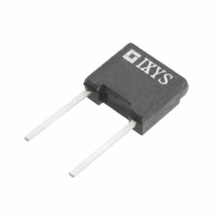
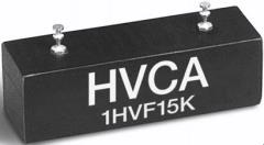
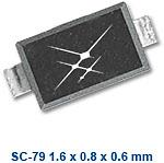
High Voltage Diodes Media Gallery
Standards
- BS 9300 C124-126 — Detail specification for silicon high-voltage rectifier diodes.
- BS 9300 C432 — Detail specification for silicon high-voltage diodes.
- BS 9300 C589-590 — Detail specification for silicon high-voltage diodes.
- BS 9300 C734 — Detail specification for silicon high-voltage diodes.
- BS C588 — Detail specification for silicon high-voltage diodes.
References
GlobalSpec—Robotics
GlobalSpec—Types of Diodes, Their Characteristics and Applications
GlobalSpec—Varactor Diodes
Image Credits:
IXYS Corporation | HV Components/CKE | Skyworks Solutions, Inc.