 | This up-to-date text/reference is designed to present the fundamental principles of robotics with a strong emphasis on engineering applications and industrial solutions based on robotic technology. It can be used by practicing engineers and scientists - or as a text in standard university courses in robotics. The book has extensive coverage of the major robotic classifications, including Wheeled Mobile Robots, Legged Robots, and the Robotic Manipulator. A central theme is the importance of kinematics to robotic principles. The book is accompanied by a CD-ROM with MATLAB simulations, photographs, tutorials, and third-party software (see About the CD-ROM section). |
Robotics
3.2.5 Diodes
In electronics, a diode is a component that restricts the direction of movement of charge carriers. Essentially, it allows an electric current to flow in one direction, but blocks it in the opposite direction. Today the most common diodes are made from semiconductor materials such as silicon or germanium.
Semiconductor Diodes
Most modern diodes are based on semiconductor P-N junctions. In a P-N diode,
conventional current can flow from the P-type side (the anode) to the N-type

FIGURE 3.12 Diode schematic symbol.
However, the depletion width cannot grow without limit. For each electron-hole pair that recombines, a positively charged dopant ion is left behind in the N-doped region, and a negatively charged dopant ion is left behind in the P-doped region. As recombination proceeds and more ions are created, an increasing electric field develops through the depletion zone which acts to slow and then finally stop recombination. At this point, there is a built-in potential across the depletion zone.
If an external voltage is placed across the diode with the same polarity as the built-in potential, the depletion zone continues to act as an insulator preventing a significant electric current. This is the reverse bias phenomenon. However, if the polarity of the external voltage opposes the built-in potential, recombination can once again proceed resulting in substantial electric current through the P-N junction. For silicon diodes, the built-in potential is approximately 0.6 V. Thus, if an external current is passed through the diode, about 0.6 V will be developed across the diode such that the P-doped region is positive with respect to the N-doped region and the diode is said to be turned on as it has a forward bias.
A diode s I-V characteristic can be approximated by two regions of operation. Below a certain difference in potential between the two leads, the depletion layer has significant width, and the diode can be thought of as an open

FIGURE 3.13 I-V characteristics of a P-N junction diode (not to scale).
In a normal silicon diode at rated currents, the voltage drop across a conducting diode is approximately 0.6 to 0.7 volts. The value is different for other diode types Schottky diodes can be as low as 0.2 V and light-emitting diodes (LEDs) can be 1.4 V or more (blue LEDs can be up to 4.0 V).
Referring to the I-V characteristics image, in the reverse bias region for a normal P-N rectifier diode, the current through the device is very low (in the A range) for all reverse voltages up to a point called the peak-inverse-voltage (PIV). Beyond this point a process called reverse breakdown occurs which causes the device to be damaged along with a large increase in current. For special-purpose diodes like the avalanche or zener diodes, the concept of PIV is not applicable since they have a deliberate breakdown beyond a known reverse current such that the reverse voltage is clamped to a known value (called the zener voltage or breakdown voltage). These devices, however, have a maximum limit to the current and power in the zener or avalanche region.
Zener Diode
Refer to the characteristic curve of a typical rectifier (diode) in Figure 3.14. The forward characteristic of the curve we have previously described above in the diode section. It is the reverse characteristics we will discuss here.

FIGURE 3.14 Current-voltage characteristics of a typical P-N junction.
Notice that as the reverse voltage is increased the leakage current remains essentially constant until the breakdown voltage is reached where the current increases dramatically. This breakdown voltage is the zener voltage for zener diodes. While for the conventional rectifier or diode it is imperative to operate below this voltage; the zener diode is intended to operate at that voltage, and so finds its greatest application as a voltage regulator.
The basic parameters of a zener diode are:| (a) | Obviously, the zener voltage must be specified. The most common range of zener voltage is 3.3 volts to 75 volts; however voltages out of this range are available. | |
| (b) | A tolerance of the specified voltage must be stated. While the most popular tolerances are 5% and 10%, more precision tolerances as low as 0.05% are available. A test current (Iz) must be specified with the voltage and tolerance. | |
| (c) | The power-handling capability must be specified for the zener diode. Popular power ranges are: 1/4, 1/2, 1, 5, 10, and 50 watts. |
Varactor Diode
The varactor diode symbol is shown in Figure 3.15 with a diagram representation. When a reverse voltage is applied to a P-N junction, the holes in the Pregion are attracted to the anode terminal and electrons in the N-region are attracted to the cathode terminal creating a region where there is little current.

FIGURE 3.15 (a) Varactor diode symbol and (b) its diagram representation.
This region, the depletion region, is essentially devoid of carriers and behaves as the dielectric of a capacitor.
The depletion region increases as the reverse voltage across it increases; and since capacitance varies inversely as dielectric thickness, the junction capacitance will decrease as the voltage across the P-N junction increases. So by varying the reverse voltage across a P-N junction the junction capacitance can be varied. This is shown in the typical varactor voltage-capacitance curve below in Figure 3.16.
Notice the nonlinear increase in capacitance as the reverse voltage is decreased. This nonlinearity allows the varactor to also be used as a harmonic generator.
Major varactor considerations are:
(a) Capacitance value
(b) Voltage
(c) Variation in capacitance with voltage
(d) Maximum working voltage
(e) Leakage current

FIGURE 3.16 Varactor voltage-capacitance curve.
Tunnel Diode and Back Diode
Tunnel Diode
A tunnel diode is a semiconductor with a negative resistance region that results
in very fast switching speeds, up to 5 GHz. The operation depends upon
a quantum mechanic principle known as tunneling wherein the intrinsic
voltage barrier (0.3 volt for germanium junctions) is reduced due to doping
levels which enhance tunneling. Referring to the curves below, superimposing
the tunneling characteristic upon a conventional P-N junction, we show
in Figure 3.17:

FIGURE 3.17 Combination of tunneling current
and
conventional P-N junction current resulting in
a
composite characteristic which is the tunnel
diode
characteristic curve.
The negative resistance region is the important characteristic for the tunnel diode. In this region, as the voltage is increased, the current decreases; just the opposite of a conventional diode. The most important specifications for the tunnel diode are the Peak Voltage (Vp), Peak Current (Ip), Valley Voltage (Vv), and Valley Current (Iv).
Back Diode
A back diode is a tunnel diode with a suppressed Ip and so approximates a conventional
diode characteristic. See the comparison in the figures below:

FIGURE 3.18
TABLE 3.1 Typical Tunnel Diodes Supplied by American Microsemiconductor | |||||||||
|---|---|---|---|---|---|---|---|---|---|
| Part Number | Ip Peak Point Current (mA) | IV Valley Point Current Max. | C Capaci- tance Max. (pF) (mA) | VP Peak Point Voltage Typ. (mV) | VV Valley Voltage Typ. (mV) (mV) | Vf p Forward Peak Voltage Typ. (GHz) | RS Series Resist. Max. (ohms) | -G Nega- tive Conduc- tance (mhosx-10-3) | fRO Resis- tive Cutoff Frequ- ency Typ. |
| 1N3712 | 1.0 + 10% | 0.18 | 10 | 65 | 350 | 500 | 4.0 | 8 Typ. | 2.3 |
| 1N3713 | 1.0 + 2.5% | 0.14 | 5 | 65 | 350 | 510 | 4.0 | 8.5 + 1 | 3.2 |
| 1N3714 | 2.2 + 10% | 0.48 | 25 | 65 | 350 | 500 | 3.0 | 18 Typ | 2.2 |
| 1N3715 | 2.2 + 2.5% | 0.31 | 10 | 65 | 350 | 510 | 3.0 | 19 + 3 | 3.0 |
| 1N3716 | 4.7 + 10% | 1.04 | 50 | 65 | 350 | 500 | 2.0 | 40 Typ. | 1.8 |
| 1N3717 | 4.7 + 2.5% | 0.60 | 25 | 65 | 350 | 510 | 2.0 | 41 + 5 | 3.4 |
| 1N3718 | 10.0 + 10% | 2.20 | 90 | 65 | 350 | 500 | 1.5 | 80 Typ. | 1.6 |
| 1N3719 | 10.0 + 2.5% | 1.40 | 50 | 65 | 350 | 510 | 1.5 | 85 + 10 | 2.8 |
| 1N3720 | 22.0 + 10% | 4.80 | 150 | 65 | 350 | 500 | 1.0 | 180 Typ. | 1.6 |
| 1N3721 | 22.0 + 2.5% | 3.10 | 100 | 65 | 350 | 510 | 1.0 | 190 + 30 | 2.6 |
TABLE 3.2 Typical Ultra-high-speed Switching Tunnel Diodes Supplied by American
Microsemiconductor | ||||||||
|---|---|---|---|---|---|---|---|---|
| Part Number | Ip Peak Point Current (mA) | IV Valley Point Current Max. | C Capaci- tance Max. (pF) Max. (mV) | VP Peak Point Voltage (mV) | VV Valley Voltage Typical I (mV) | Vf p Forward Voltage Typica Typical | RS Series Resist. Typical (ohms) | T Rise Time Typical (psec.) |
| TD-261 | 2.2 ± 10% | 0.31 | 3.0 | 70 | 390 | 500-700 | 5.0 | 430 |
| TD-261A | 2.2 ± 10% | 0.31 | 1.0 | 80 | 390 | 500-700 | 7.0 | 160 |
| TD-262 | 4.7 ± 10% | 0.60 | 6.0 | 80 | 390 | 500-700 | 3.5 | 320 |
| TD-262A | 4.7 ± 10% | 0.60 | 1.0 | 90 | 400 | 500-700 | 1.7 | 350 |
| TD-263 | 10.0 ± 10% | 1.40 | 9.0 | 75 | 400 | 500-700 | 1.7 | 350 |
| TD-263A | 10.0 ± 10% | 1.40 | 5.0 | 80 | 410 | 520-700 | 2.0 | 190 |
| TD-263B | 10.0 ± 10% | 1.40 | 2.0 | 90 | 420 | 550-700 | 2.5 | 68 |
| TD-264 | 22.0 ± 10% | 3.80 | 18.0 | 90 | 425 | 600 Typ. | 1.8 | 185 |
| TD-264A | 22.0 ± 10% | 3.80 | 4.0 | 100 | 425 | 550-700 | 2.0 | 64 |
| TD-265 | 50.0 ± 10% | 8.50 | 25.0 | 110 | 425 | 625 Typ. | 1.4 | 100 |
| TD-265A | 50.0 ± 10% | 8.50 | 5.0 | 130 | 425 | 640 Typ. | 1.5 | 35 |
| TD-266 | 100 ± 10% | 17.50 | 35.0 | 150 | 450 | 650 Typ. | 1.1 | 57 |
| TD-266A | 100 ± 10% | 17.50 | 6.0 | 180 | 450 | 650 Typ. | 1.2 | 22 |
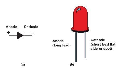
FIGURE 3.19 (a) LED symbol. (b) LED diagram.
© 2006-2026 Infinity Science Press. All rights reserved.